PCB Layout Services
PCB Layout is a process of planning, placement and routing PCB design on a layout software, according to schematic, BOM, mechanical specifications and other instructions provided by customer, and sometimes, we simply call it PCB routing. PCB layout is different from PCB design, PCB design is a more complex process including BOM preparation, schematic capture, PCB layout and etc.
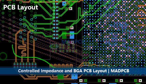
PCB Layout
Through many years of experience and continuous exchange with manufacturing specialists from PCB and assembly manufacturer MADPCB, PCB layouts are designed to pass all stages of production without problems. Product quality and reliability are increased by appropriate adjustments to production processes, while costs are usually reduced by avoiding unnecessary or complicated production steps.
PCB Layout by Manual, Not by Software
The work of PCB layout or routing at MADPCB is taken over by the layout engineers but not by the software. The skilled PCB layout engineers with theoretical background knowledge finds the ideal patch between high-speed, high components density, fine line technology, EMC-compliant design and -which is becoming increasingly important -even the heat management on the PCB. By doing so, the cost-efficient manufacturing and assembly of printed circuit boards (PCB) is not lost slight of. Due to the close link between development and production, new designs, footprints or whole technologies pass through a special control mechanism. If necessary, they are improved in iterative steps until they have reached a reliable maturity. Of course, it is not always about the high density interconnect (HDI), which is adjusted for its runtime. Even for simple PCB layouts, the choosing of appropriate technology and design leads to a high savings potential. Your benefits from this process, whether double-sided or multilayered, square, round or otherwise shaped board, HDI, high frequency and impedance controlled, MADPCB brings your expectations and specifications into appropriate housing.
PCB Layout Steps
There are a number of steps that should be followed in any PCB layout process.
- Initial Settings: This stage of the PCB layout involves setting up the snap and visible grids. At this stage, the default trace and pad sizes should also be determined and set.
- Mechanical Elements: importing PCB outline to limit the routing space, and any reference marks and holes, which may be required for PCB fabrication machines, SMT pick-and-place machines, or test fixtures.
- Components Placement: all components on the BOM need to be placed onto the PCB, then they are available for moving and setting in place later.
- Functional Blocks: Relevant components should be moved into their functional blocks, then associated components are close to each other and the circuit can be routed easily later.
- Identifying and Routing Critical Traces: Critical traces should be identified and routed as required first, then the remained of the design can be implemented around these traces rather than trying to resolve problems in later layout.
- Power and Ground Routing: Power and Ground layers are often included as plane, occupying a complete layer of the PCB. By doing so, there are advantages not only in terms of enabling the higher levels of current to be routed easily, but it also significantly reduces any problems with interference on the PCB.
- Remaining Lines Routing: Remaining lines can be routed by software (through auto routing function) or by manual. If adopt auto routing, need to set up various parameters to ensure the PCB layout is compliant to the requirements.
- Final Lines Routed by Manual: If auto-routing completed, maybe there are some traces would not route. These final traces need to be routed manually. If the layout design has become too complicated for space and the available number of layers, it may be necessary to make some fundamental changes to the layout still by manual.
- Final Layout Adjustment: Once all lines have been routed, it is complete any small items that may need completing at this stage. Upon requirements, do the final layout adjustment.
- Running DRC: Running Design Rules Check (DRC) at this stage to catch any problems rather than once a prototype PCB assembly has been built.
- Data Outputs: When layout and check complete, it’s time to output documentations for PCB and assembly prototyping, which is used for verifying whether the design is ok.