Table of Contents
HDI Printed Circuit Board (PCB)
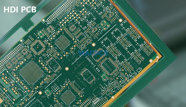
What’s HDI PCB? High-density interconnect (HDI) PCBs are characterized by finer lines, closer spaces, and more dense wiring, which allow for a faster connection while reducing the size and bulk of a project. These boards also feature blind and buried vias, laser ablated microvias, sequential lamination, and via in-pads.
As a result, a HDI board can house the functionality of the previous boards used. MADPCB is an HDI PCB manufacturer and provider in Shenzhen, China supports HDI PCB prototype and mass production with less expensive price and quick-turn lead time. Customers from a variety of industries we serve have a common that have high expectations in quality, reliability and on-time delivery in HDI PCB production. Our quality is not afterthought, but built into each process from front-end to fabrication and shipping.
HDI PCB Manufacturing Process
The overall process for manufacturing HDI PCB is essentially the same as for fabricating other PCB board, with notable differences for PCB stack-up and hole drilling. Since HDI boards generally require smaller drill holes for vias, laser drilling is usually required. Although laser drills can produce smaller and more precise holes, they are limited by depth. Therefore, a limited number of layers can be drilled through at a time. For HDI boards, which are invariably multilayer and may contain buried and blind vias, multiple drilling processes may be required. This necessitates successive layer boding to achieve the desired stack-up or sequential lamination cycles. Not surprisingly, this can significantly increase PCB manufacturing time and cost.
HDI PCB fabrication is an advanced technology and therefore requires expertise along with specialized equipment like laser drills, laser direct imaging (LDI) capability, and special clean room environments. In order to efficiently manufacture high-quality and reliable HDI PCB products, you must understand the HDI board manufacturing process and coordinate with your HDI PCB supplier to implement good DFM (Design for Manufacturability) for HDI layout design.
Click to check our PCB Fabrication Process and PCB Capabilities
HDI PCB Design
The electronics industry is largely consumer-driven and the directive for smaller more capable products with increased functionality will only intensify in the years to come. At MADPCB, we are well-positioned to assist you in meeting this demand with advanced equipment, processes and expertise to manufacture your HDI PCB boards quickly and precisely.
HDI, with its attendant reduction in size and weight, goes hand in hand with this greater density of surface mount components. Of course, the high count connections for integrated circuits and components including BGAs and flip chips simply adds to the need for HDI. Because of fine lines and blind microvias design, the dimple and bump after via filling are the two parameters to check whether the HDI printed boards reach your thin copper deposited requirement. HDI layout always refer to DDR3, DDR4, XAUI, PCIe, LVDs, Gig-E applications, the designs always include high-speed stripline and microstrip, your PCB fabricator should have advanced manufacturing capabilities.
HDI Board Stack-up
- 1+N+1 with laser microvia and mechanical buried core via. The “1” represents “build-up” or sequential lamination on each side of the core.
- i+N+i (i>=2) – PCBs contain 2 or more “build-up” of high-density interconnect layers. Microvias on different layers can be staggered or stacked. Copper filled stacked microvia structures are commonly seen in challenging designs.
- Any Layer HDI (ELIC) – All the layers of a PCB are high-density interconnection layers which allows the conductors on any layer of the PCB to be interconnected freely with copper filled stacked microvia structures (“any layer via”). This provides a reliable interconnect solution for highly complex large pin-count devices, such as CPU and GPU chips utilized on handheld and mobile devices.
HDI PCB Types
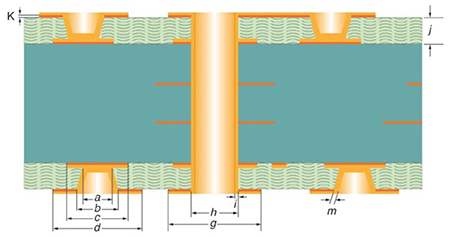
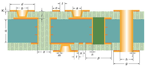
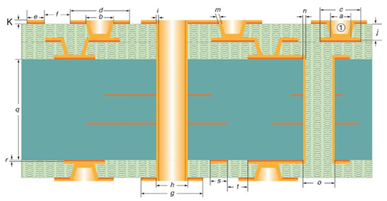
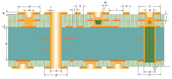


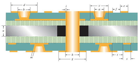
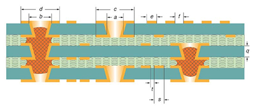
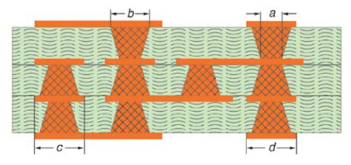
When it comes to the HDI board construction, we have to talk about HDI PCB types. There are 6 different HDI PCB types, including Type I (1 [C] 0 or 1 [C] 1), Type II (≥2[C] 0 or 1 [C] 1), Type III (≥2 [C]≥0), Type IV (≥1 [P]≥0), Type V (Coreless (Layer Pairs)) and Type VI (any layer).
| Type | Core / Passive | Definition |
| Type I | 1 [C] 0 or 1 [C] 1 | Type I construction describes an HDI board in which there are both microvias and conductive vias used for interconnection. Type I constructions describe the fabrication of a single microvia layer on either one (1 [C] 0) or both (1 [C] 1) sides of a PCB substrate core. |
| Type II | ≥2[C] 0 or 1 [C] 1 | Type II construction describes an HDI PCB in which there are plated microvias, plated buried vias, and may have PTHs used for surface-to-surface interconnection. The buried vias may be prefilled with a conductive/non-conductive paste or partially or completely filled with dielectric material from the lamination process. |
| Type III | ≥2 [C]≥0 | Type III construction describes an HDI PCB board in which there are plated microvias, plated buried vias, and may have PTHs used for surface-to-surface interconnection. The buried vias may be prefilled with a conductive/non-conductive paste or partially or completely filled with dielectric material from the lamination process. |
| Type IV | ≥1 [P]≥0 | Type IV construction describes an HDI circuit board in which the microvia layers are used over an existing predrilled passive substrate. Additional microvia layers can be added sequentially. The core substrate is usually manufactured using conventional printed board techniques. The function of the core is passive, yet it may be used for thermal, CTE management, or shielding (the core doesn’t perform an electrical function). |
| Type V | Coreless
(Layer Pairs) |
Type V construction describes an HDI printed circuit board in which there are both plated microvias and conductive paste interconnections through a co-lamination process. There is essentially no core to this type of construction since all layer pairs have the same characteristics. Type V construction consists of the HDI PCB fabrication of an even number of layers that are laminated together at the same time the interconnections are made between the odd and even layers. This type of construction is neither build-up nor sequential; it it a single lamination process. |
| Type VI | Any Layer | Type VI construction describes an HDI printed board in which the electrical interconnection and mechanical structure are formed simultaneously. The layers may be formed sequentially or co-laminated, and the conductive interconnection may be formed by means other than electroplating (i.e. anisotrophic films/pastes, conductive paste, dielectric piercing posts, etc.) |
Laser Drilling Technology
Unlike mechanical drills, the laser drilling process doesn’t physically contact the PCB material that it is working with. Drilling the smallest of microvias allows for more technology on the PCB surface. The high influence beam of the UV laser machine can drill through copper and organic dielectric (PP, epoxy resin, adhesive, PI, EMI shielding film and etc.) to create the tiny via hole. The UV laser has excellent reflection, absorption and transmission capacity on different materials. HDI PCBs always have a large laser drilling quantity per square meter, even more than 50K density since its high-density interconnection, and the laser machine drilling capacity always reaches 4.3million pieces daily.
Laser Direct Imaging (LDI) Technology
Imaging fine or ultra-fine traces than ever before to process these HDI boards is costly but necessary. Finer traces, spacing and annular ring requires much tighter controls. With use of finer traces, touch up rework or repair becomes an impossible task. Photo tool quality, laminate prepreg and imaging parameters are necessary for successful process. LDI (laser direct imaging) is a far better option for such fine traces and spacings. Laser direct imaging (LDI) capabilities ensure exacting registration and all multilayer inner cores receive a thorough check using Automated Optical Inspection (AOI) units for excellent defect detection of the finest features.
HDI PCB Materials Selection
Material type and construction is extremely important in designing and manufacturing HDI PCB boards. Designing HDI interconnects involves an understanding of the potential problems arising when specifying glass reinforced dielectric materials.
Microvia dielectric materials can introduce misregistration and rough vias whether plasma, laser, or mechanical drilling is performed. Not only are the material properties of the microvia dielectric materials called into question, but also the consistency of the weave, as well as the quality of the fibers used. The potential to close the weave openings by spreading the fibers out is extremely important, as this minimizes open spaces that cause skew and drift.
- Copper Clad Laminate (CCL): Copper clad laminate materials have copper foil laminated onto one or both sides of cured (C-stage) dielectric. The rigid CCLs can be FR4, FR-5 or some PTFE. The typical application uses single-side clad laminate material where the copper clad is used as the outer layer and the c-stage is bonded to the sub-composite. Microvias are formed utilizing laser drilling methods. Materials available differ by reinforcement (woven glass, non-woven glass and expanded PTFE) and chemistries involved (epoxies, polyimide, polyester etc.).
- Resin Coated Copper (RCC): Resin coated copper materials are compromised of copper foil, coated with a resin dielectric material that can be directly bonded to the sub-composite. They differ by whether they are wet processable or not. In non-wet processable-coated copper materials, microvias are formed utilizing plasma or laser drilling methods.
- PP: Prepreg, also referred to B-stage, Bonding sheet, or simply Preg, which is composited of fiberglass fabric impregnated with resin. The resin has been partially cured but not hardened during the Prepreg coating operation. When heating the PCB stack-up in pressing process, the resin in PP will flow, stick and bond the PCB core with copper foil or other materials.
Typical Feature Sizes for HDI PCB Construction, μm [mil]
| ASPECT RATIO | Level A | Level B | Level C | |
| Microvia plating aspect ratio |
≤0.5:1 (K + j) / b |
>0.5:1 to 0.85:1
(K + j) / b |
>0.85:1 (K + j) / b |
|
| Through via hole aspect ratio3 |
≤8:1 (2K + u) / h |
>8:1 to 10:1
(2K + u) / h |
>10:1 (2K + u) / h |
|
| Buried via aspect ratio3 |
≤8:1 (2r + q) / h |
>8:1 to 10:1
(2r + q) / h |
>10:1 (2r + q) / h |
|
| Symbol | Feature | Level A | Level B | Level C |
| a | Microvia diameter at target land
(as formed, no plating) |
≥b/2 | ≥b/2 | ≥b/2 |
| b | Microvia diameter at capture land
(as formed, no plating) |
150μm [6mil] | 100μm [4mil] | 75μm [3mil] |
|
c4 Process 2 from Figure 9-1 |
Microvia target land size =
[(b + 2X min annular ring) + FA(1)] |
300μm [12mil] | 225μm [9mil] | 175μm [7mil] |
| Microvia FA | 150μm [6mil] | 125μm [5mil] | 100μm [4mil] | |
|
d4 Process 2 from Figure 9-1 |
Microvia capture land size =
[(b + 2X min annular ring) + FA(1)] |
300μm [12mil] | 225μm [9mil] | 175μm [7mil] |
| s | Print & Etch conductor trace width | 100μm [4mil] | 60μm [2.4mil] | 50μm [2mil] |
| t | Print & Etch conductor spacing | 100μm [4mil] | 75μm [3mil] | 50μm [2mil] |
| e5 | Plated conductor trace width | 100μm [4mil] | 75μm [3mil] | 50μm [2mil] |
| f5 | Plated conductor spacing | 100μm [4mil] | 90μm [3.5mil] | 60μm [2.4mil] |
| g | Through via land size =
[(h + 2X min annular ring) + FA(1)] |
See 9.1.1 of IPC-2221 | See 9.1.1 of IPC-2221 | See 9.1.1 of IPC-2221 |
| h | Through via diameter
(as formed, no plating) |
See Table 5-2 | See Table 5-2 | See Table 5-2 |
| i | Min thru via hole wall plating thickness | See IPC-2221, Table 4-3 | See IPC-2221, Table 4-3 | See IPC-2221, Table 4-3 |
| j | Dielectric thickness
(HDI blind microvia layer)(2) |
64μm [2.5mil] | 64μm [2.5mil] | <50μm [2mil] |
| k | Cu foil thickness to be Plated
(this represents the max foil thickness to achieve features “e” and “f” for one plating step) |
1/2oz (See IPC-2221, Table 10-2) |
1/4oz
(See IPC-2221, Table 10-2) |
1/8oz (See IPC-2221, Table 10-2) |
| k’ | Cu foil thickness for Print & Etch
(this represents the max foil thickness to achieve features “e” and “f” for one plating step) |
1/2oz (See IPC-2221, Table 10-1) |
1/3oz
(See IPC-2221, Table 10-1) |
1/4oz (See IPC-2221, Table 10-1) |
| K | Total Copper Thickness at drill | K + plating present at drill | ||
| m | Min blind microvia hole plating thickness | 12μm [4.7mil] | 12μm [4.7mil] | 12μm [4.7mil] |
| m’ | Min buried microvia hole plating thickness | 12μm [4.7mil] | 12μm [4.7mil] | 12μm [4.7mil] |
| n | Min buried via hole wall plating thickness |
See IPC-2221 Table 4-3 |
See IPC-2221
Table 4-3 |
See IPC-2221 Table 4-3 |
| o | Buried via diameter
(as formed, no plating) |
See IPC-2221 Table 9-4 |
See IPC-2221 Table 9-4 |
See IPC-2221 Table 9-4 |
| p | Buried via land size =
[(o + 2X annular ring) + FA(1)] |
See 9.1.1 of IPC-2221 | See 9.1.1 of IPC-2221 | See 9.1.1 of IPC-2221 |
| q | Buried via core thickness =
[(o + 2X annular ring) + FA(1)] |
75μm[3mil] | 50μm[2mil] | <50μm[2mil] |
| r | Buried via Cu foil thickness
(outermost layer) |
1/2oz (See IPC-2221, Table 10-2) |
1/4oz (See IPC-2221, Table 10-2) |
1/8oz (See IPC-2221, Table 10-2) |
| u | Core board thickness
(excluding conductors) |
75μm[3mil] | 50μm[2mil] | <50μm[2mil] |
Note 1. FA = Fabrication Allowance which considers production master tooling and process variations required to fabricate printed circuit boards.
Note 2. Measured from top surface of Layer 2 Cu to bottom surface of Layer 1 Cu.
Note 3. Aspect Ratio ≥8:1 are not recommended for hole sizes less than 0.25mm [9.8mil] diameter.
Note 4. For process 1 described in Figure 9-1, Level A should be increased by 100μm [4mil] and Level B and Level C are not recommended.
HDI PCB Manufacturer
MADPCB is a reliable HDI PCB manufacturer China, has highly skilled engineers to partner with our customers for achieving economical perfection in manufacturing any type of multi-layer boards, rigid-flex or HDI boards of any complexity. Contact us today to learn more about HDI PCB and how we can provide your company with the most highly complex HDI printed circuit boards designed and manufactured in the market.

