What’s PCI Express?
Peripheral Component Interconnect (PCI) Express, officially abbreviated as PCIe or PCI-e, is a high-speed serial computer expansion bus standard, designed to replace the older PCI, PCI-X and AGP bus standards. It is the common motherboard interface for personal computers’ graphics cards, hard disk drive host adapters, SSDs, Wi-Fi and Ethernet hardware connections.
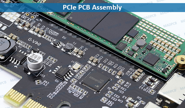
PCIe PCB Assembly
It was introduced in 1992 with the aim of supporting complex data transfers and evolved its purpose way beyond the same. The PCI bus was made to be available in 32-bit and 64-bit versions. The PCI technology has undergone various updates to evolve into PCI Express which is still under development.
There exist the PC-AT Standard (also called “ISA”) with a pitch of 2.54mm (0.1 inch) and the PCI standard with a grid spacing of 1.27mm (0.05 inch) for the gold fingers. Additionally, there are PCIe cards with 1.0mm and Mini PCB Express cards (mPCIe) with 0.8mm pitch.
PCIe currently comes in four different generations: PCIe 1.0, PCIe 2.0, PCIe 3.0 and PCIe 4.0. The bandwidth doubles with each generation. Given below are the detailed specifications of the PCIe generations.
| PCI Express Version |
Transfer Rate | x1 Throughput |
x4 Throughput |
x8 Throughput |
x16 Throughput |
| 1 | 2.5 GT/s | 250 MB/s | 1.0 GB/s | 2.0 GB/s | 4.0 GB/s |
| 2 | 5 GT/s | 500 MB/s | 2.0 GB/s | 4.0 GB/s | 8.0 GB/s |
| 3 | 8 GT/s | 984.6 MB/s | 3.94 GB/s | 7.88 GB/s | 15.8 GB/s |
| 4 | 16 GT/s | 1969 MB/s | 7.88 GB/s | 15.75 GB/s | 31.5 GB/s |
PCI Express Design Guidelines
Trace Routing specifications
When compared to most high-speed devices available, PCIe generations permit longer trace in their layout routing specs. Every generation comes with its own specifications on impedance and maximum trace lengths for varying data transfer rates. These should be closely followed to obtain the required performance. The exact routing specifications will depend on which PCIe generation you are utilizing for your design.
Trace lengths in Gen 1 and Gen 2 both let RX (received) and TX (transmitted) signal traces reach up to 21 inches in length. When it comes to Gen 3, trace lengths can only go up to 14 inches on signal trace PCIe planes. While each TX trace pair can have only two vias, RX pairs can include up to four vias to maintain impedance within the required specification. A COM Express carrier board allows for trace lengths of up to 9 inches for Gen 1 and 2 when the traces are being sent to a PCIe slot.
The differential impedance of signal lines depends on the bus used to connect to the PCIe board.
| Type of PCB | Differential Impedance (Ohm) |
| Standard PCB | 100 |
| PCI-SIG bus Gen 1 | 85 |
| PCI-SIG bus Gen 2 | 85 |
| PCI-SIG bus Gen 3 | 85 |
| COMCDG Rev. 1.0 bus Gen 1 PCIe | 92 |
| COMCDG Rev. 1.0 bus Gen 2 PCIe | 92 |
| COMCDG Rev. 2.0 bus Gen 3 PCIe | 85 |
The tolerance for differential impedance values also differs among the various PCIe generations and bus standards. The values may be different for each bus and generation combination, but they can be found in the COMCDG Rev. 2.0 specification. When keeping the impedance of microstrip traces within specified tolerances, you need to use PCB design software to include controlled impedance routing features. The interactive routing tool in the software will ensure your traces are spread out with the right spacing and geometry.
Stack-up and Grounding
Standard PCIe boards incorporate a 4-layer stack-up with two interior power planes and two signal layers on each surface. Each power layer can be brought to varying bias levels based on device requirements. Other designs for PCIe boards go for a 6-layer stack-up with two signal layers that run between two power layers. In another scenario, one of the power planes can be replaced with a ground plane. In both cases, you can achieve better immunity to EMI by routing signal traces on the inner layers.
You can even route traces with varying data rates on different layers. For instance, in a mixed-signal board such as the ones in a Wi-Fi device on a PCIe card, you can route digital traces on the outer layers and the RF traces on the inner layers. The power / ground planes will effectively block noise from reaching the sensitive analog signal traces.
Regardless of the stack-up used, you will need to meet the overall board thickness standard of 1.57 mm or 1 mm for PCIe Mini. You will also need to consider standard high-speed design techniques as the Gen 1 of PCIe operates at 2.5 GHz clock speed with future generations increasing in speed.
PCIe Differential Pair Routing
Routing around obstructions and component placement and via placement on a PCIe board is really important. There needs symmetric routing to pins, pads, and components along with the BGA breakout routing. Differential pairs need to be tightly coupled throughout their entire length, with variations in one trace due to vias, pads, or components being mirrored in the other trace. This ensures crosstalk is minimized throughout the differential pair length. Similar practices need to be applied while routing BGA breakouts or breakouts from other components.
Others
- The entire plug area including the gold fingers must not be covered by solder-stop (see diagram)
- Plated-through holes within the contact area are not allowed
- The circuit board surface may be freely selected
- The gold fingers are manufactured using “hard gold” (electroplated gold), Au thickness 0.8 – 2µm
|
Technical Parameter |
PC card | PCI card | PCIe card |
mPCIe card |
|
Pitch |
2.54mm | 1.27mm | 1.0mm | 0.8mm |
|
Thickness |
1.6mm | 1.6mm | 1.6mm |
1.0mm |
|
Chamfer angle |
45° | 20° | 20° | 20°/45° |
|
Spacing gold fingers / PCB contour |
0.7mm | 2.0mm | 1.4mm |
0.5mm/0.25mm |
For customer-specific applications, a 30° chamfer angle can also be selected.
As the performance requirements of high-speed PCB design continue to increase, it becomes critical to ensure that your design meets PCIe layout routing specifications. PCB manufacturing for PCIe requires a great deal of expertise and experience that only a few manufacturers can provide. Welcome to ask a quick quote on your next PCI Express PCB and assembly projects from MADPCB.