Table of Contents
Solder Mask on PCB
Solder Mask, Soldermask or Solder Resist is a thin protective lacquer-like polymer coating that is usually applied to the copper traces of a bare printed circuit board (PCB) for protection against oxidation, and to prevent solder bridges from forming between closely spaced solder pads. Once applied, solder mask openings must be formed for components terminal soldering.
Soldermask Relief and Soldermask Dam
There are two main solder mask types,
- Liquid Photo-Imageable (LPI) Solder Mask (or LPSM) ink
- Dry Film Photo-Imageable Solder Mask (DFSM) Ink.
LPI solder mask can be silkscreened on the PCB, exposed to the pattern and developed to provide window openings in the pattern for parts to be soldered to the copper pads. DFSM is vacuum-laminated on the PCB then exposed and developed. All two processes typically go through a thermal cure of some type after the pattern is defined although LPI solder masks are also available in ultra violet (UV) cure.
In the past, solder masks were applied in dry film sheets, but with the advent of LPI solder masks and techniques, DFSM is rarely used today. MADPCB uses LPI (Liquid Photo Imageable) solder masks. LPI masks are by far the most common type of mask used today. They are more reliable, can be printed very accurately, and make better contact with the surface of the board and the copper features on which they’re applied to protect. LPI solder masks are an epoxy-based material so they are very durable and nearly impossible to remove once they have been cured.
How to Apply LPI Solder Mask on Printed Boards?
Liquid Photo Imageable solder mask is applied to your board in the following steps:
- The PCB production panel is thoroughly cleaned to ensure no dust particles are trapped under the solder mask.
- The panels are completely covered on single or double sides with the LPI solder mask.
- The coated panels are placed in an oven to tack-dry the solder mask just enough to finish processing.
- A film is made of your solder mask Gerber files, one for each side of the board. Where you want solder mask to stick to the board, the film will be clear. Where the mask should be removed will be black on the film.
- The tack-dried boards are placed into a UV developer and the film is precisely aligned over the board. The blacked-out locations on the film will prevent the UV light from curing the mask where it is not wanted.
How to Define Solder Mask Layer(s) in Gerber Data?
Solder Mask Layers in Gerber data should be thought of as a negative image. This means where you see color on the mask layer is where no mask coverage. Everywhere else will be covered with solder mask. Think of the solder mask as completely covering your PCB board and the solder mask files show the places where no solder mask applied.
- In Gerber data of rigid boards, GTS is Top Soldermask layer and GBS is Bottom Soldermask layer.
- In Gerber data of flex or rigid-flex PCBs, GTS and GBS can be both soldermask and coverlay layers.
During the working Gerber files issuing (CAM engineering) process, MADPCB will automatically adjust your solder mask apertures as needed for PCB production. Generally, a solder mask aperture will be adjusted so it is 4mil larger than the copper pad it is exposing (2mil larger per side). If we printed the mask exactly the same size as the copper pad, there is a good chance the mask would not be exactly centered on pad which would result in some of your copper pad being covered with solder mask. The tolerance for solder mask registration is +/-2mil, and that’s why we adjust apertures to be 2mil larger all the way around the copper feature helping to ensure the entire pad can be soldered.
There are times when a solder mask defined (SMD) pad is required. A SMD pad is when the solder mask relief is the same size or smaller than the copper pad it is exposing. These are generally used when solder mask dams are needed between surface mount devices’ pads, but there is not enough space print a dam and follow the standard soldermask swell. If you require a soldermask defined pad and do not wish solder mask clearances to be modified, you must include a fab note stating which pads should not be adjusted.
Solder Mask and PCB Assembly
Solder mask is very important when it comes to PCB assembly no matter with reflow or wave soldering techniques. As a reliable PCB assembly manufacturer, MADPCB always puts solder mask dams between your surface mount pads if it’s possible. This helps prevent accidental solder bridging during PCB assembly and greatly reduces the amount of rework required to remove shorts.
Be aware there are limitations with regards to minimum Pad-to-Pad spacing so not all SMDs’ (Surface Mount Device) pads will be able to have solder mask dams between them. Here are our minimum mask dam guidelines.
Solder Mask is also used to prevent solder starvation. Solder starvation can occur for many reasons but solder mask can prevent solder from wicking away from its intended location. Open vias near your surface mount pads (such as with BGAs), can wick solder away from the pad and down the open via resulting in intermittent or no connection. Solder mask if frequently used to tent or plug these vias to prevent this. A good rule of thumb to follow is, cover everything with solder mask unless you need to solder to it or use it as a test point.
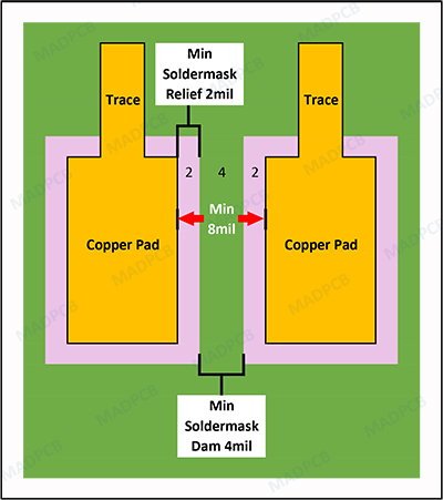
Min Solder Mask Relief and Min Solder Mask Print Width (Dam)
To ensure copper pads are not partially covered with mask, we require a min 2mil clearance between the pad and where the solder mask will be printed. If your files have a smaller soldermask clearance, MADPCB will adjust this automatically.
There is a limit to how narrow a solder mask dam can be applied and have it stick to the raw laminate. MADPCB’s print width (dam) is 4mil.
If the space between copper pads are less than 8mil, MADPCB will not be able to print soldermask between these copper features. MADPCB will adjust your files automatically to a block relief.
Solder Mask Thickness
According to IPC-SM-840D, there is no a specific solder mask thickness, like 20μm or 25μm, but has a limit on solder mask thickness:
- “3.4.1 Solder Mask Thickness The printed board fabricator shall confirm that the minimum thickness of the solder mask on the printed board is sufficient to meet the requirements of 3.8.1. The coating thickness shall be measured by any micrometer or indicator accurate to 2.5 µm [0.0001 in] or microsection prepared in accordance with IPC-TM-650, Method 2.1.1 or Method 2.1.1.2. If a specific thickness or breakdown voltage is required or allowed, it shall be AABUS (as agreed between user and supplier).”
- “3.8.1 Dielectric Strength The solder mask material shall meet or exceed the minimum value of 500 VDC per 25 µm [0.001 in] of thickness when tested in accordance with IPC-TM-650, Method 2.5.6.1. Thickness of solder mask less than 25 µm [0.001 in] shall meet an absolute minimum breakdown voltage of 500 VDC.”

Solder Mask Block Relief
At MADPCB, the average soldermask thickness we can reach ranges from 15μm to 25μm.

Solder Mask Individual Relief
IPC-SM-840D |Qualification and Performance Specification of Permanent Solder Mask
This specification provides two classes of requirements, T and H, to reflect functional performance requirements and testing severity based on industry/end use requirements. Qualification to a particular class shall not be extended to cover any other class.
- T -Telecommunication This includes computers, telecommunication equipment, sophisticated business machines, instruments, and certain noncritical military applications. Solder mask on printed boards in this class is suitable for high performance commercial and industrial products in which extended performance life is required but for which interrupted service is not life threatening.
- H -High Reliability/Military This includes that equipment where continued performance is critical, equipment down-time cannot be tolerated and/or the equipment is a life support item. Solder mask on printed boards of this class is suitable for applications where high levels of assurance are required and uninterrupted service essential.
Notes:
Class Designations -Previous versions of this and other IPC specifications make reference to “Class 1”, Class 2” and “Class 3” end product classes. For all practical purposes there is no Class 1 solder mask. The requirements in this specification are not applicable for solder mask used in Class 1 end-product. Class 2 is equivalent to Class T (Telecommunications). Class 3 is the equivalent of Class H (Military/high reliability).