Table of Contents
What’s A Microvia?
Microvia, also called Micro Via, Micro-Via, μVia or sometimes Laser Via, or Laser Ablated Via. IPC standards revised the definition of a microvia in 2013 to a hole with an aspect ratio of 1:1. Previously, microvia was any hole less than or equal to 0.15mm (6mil) in diameter.
Microvias are used as the interconnects between layers in high density interconnect (HDI) substrates and printed circuit boards (PCBs) to accommodate the high input/output (I/O) density of advanced packages. Driven by portability and wireless communications, the electronics industry strives to produce affordable, light, and reliable products with increased functionality. At the electronic component level, this translates to components with increased I/Os with smaller footprint areas (e.g. flip-chip packages, chip-scale packages, and direct chip attachments), and on the printed circuit board and package substrate level, to the use of high density interconnects (HDIs) (e.g. finer traces and spaces, and smaller vias).
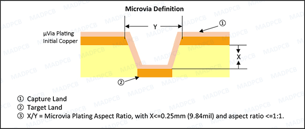
Microvia is smaller Via, both in blind and buried. Vias and Microvias are copper plated holes. There are 2 main features in micro via:
Microvia, Micro Via, μVia
- Capture Land (Microvia Top Land): Land where the microvia originates
- Target Land (Via Bottom Land): Land on which a microvia ends
And there are 3 kinds of microvias:

HDI Microvias-Staggered Microvias, Stacked Microvias &Skipped Microvias
- Stacked Microvias: A microvia formed by stacking one or more microvias on a via that provides an interlayer connection between three or more conductive layers.
- Staggered Microvias: A set of microvias, formed on two or more different layers, which are offset such that the land diameters are tangential or greater.
- Skipped Microvias: Microvias formed in one operation, penetrating two or more HDI dielectric layers and terminating at one or more different layers.
Comparisons of Staggered, Stacked and Skipped Microvias
| Microvias | Staggered | Stacked | Skipped |
| Outer Layer Surface | +++ smallest surface |
+ largest surface |
++ medium surface |
| Copper Barrel Stability | +++ shortest connection |
++ connection to copper layer |
+ largest connection |
| Plating Surface | +++ largest |
+ smallest |
++ medium |
| Lasting Time | — 2x lasting 2x registering |
— 2x lasting 1x registering |
– 1x lasting 1x registering |
| Press Cycles | — 2 |
+ 1 |
+ 1 |
| Costs | — | — | – |
Microvia Reliability
The reliability of HDI structure is one of the major constraints for its successful widespread implementation in the PCB industry. Good thermo-mechanical reliability of microvias is an essential part of HDI reliability. Many researchers and professional have studied the reliability of micro vias in HDI boards. The reliability of microvia depends on may factors such as microvia geometry parameters, dielectric material properties, and processing parameters.Microvia reliability research has focused on experimental assessment of the reliability of single-level unfilled miicrovias, as well as finite element analysis on stress/strain distributions in single-level microvias and microvia fatigue life estimation. Micro-via failures identified from the research include interfacial separation (separation between the base of the microvia and the taget pad), barrel cracks, corner/knee cracks, and target pad cracks (also preferred to as micro-via pull out). These failures result from the thermomechanical stresses caused by coefficient of thermal expansion (CTE) mismatch, in the PCB thickness direction, between the metallization in a microvia structure and the dielectric materials surrounding the metal.
Resin Filling and Copper Plating for Microvias
Filling means closing the holes with resin and grinding the surface, obtaining in this way the planarity of the following layer. Resin filling can be individually applied for buried microvias, and mutually applied for blind microvias with copper plating (cap).What’ the copper plating thickness in through holes, blind vias, buried vias, blind and buried microvias, and buried via cores? and what’s the copper cap plating thickness of filled holes? In fact, we can find the answers in the latest IPC-6012D, and please refer to following:
| Copper Plating Thickness | Class 2 | Class 3 | Class 3A* | |
| Through, Blind, Buried Vias (>2Layers) (Min) |
Wrap: | 20μm [0.79mil] | 25μm [0.98mil] | 25μm [0.98mil] |
| Thin Areas: | 18μm [0.71mil] | 20μm [0.79mil] | 25μm [0.98mil] | |
| Wrap: | 5μm [0.20mil] | 12μm [0.47mil] | 12μm [0.47mil] | |
| Through, Blind, Buried μVias (>2Layers) (Min) |
Wrap: | 12μm [0.47mil] | 12μm [0.47mil] | 20μm [0.79mil] |
| Thin Areas: | 10μm [0.39mil] | 10μm [0.39mil] | 18μm [0.71mil] | |
| Wrap: | 5μm [0.20mil] | 6μm [0.24mil] | 6μm [0.24mil] | |
| Buried Vias Core (2Layers) (Min) |
Average: | 15μm [0.59mil] | 15μm [0.59mil] | 20μm [0.79mil] |
| Thin Areas: | 13μm [0.51mil] | 13μm [0.51mil] | 18μm [0.71mil] | |
| Wrap: | 5μm [0.19mil] | 7μm [0.27mil] | 7μm [0.27mil] | |
| Cap Plating of Filled Holes | Min: | 5μm [0.19mil] | 12μm [4.7mil] | 76μm [3mil]-General 50μm [2mil]-BGA |
| Max: | 127μm [5mil] | 76μm [3mil] | 50μm [2mil] | |
For more information about vias and micro vias treatment, please check Vias Protection.
Microvia Design
It is important to note that the land size for a microvia feature is determined, rather than simply selected, as discussed in the following.
HDI PCB manufacturers successfully use a wide variety of dielectrics for microvia boards, ranging from conventional glass reinforced epoxy to ultra-thin unreinforced materials such as resin coated copper foil (RCC). The product’s end-use environment and expected operating life, plus certain needed board-level attributes (e.g., dielectric withstand voltage, resin content to fill buried vias or avoid resin starvation, etc.) may require a particular dielectric type and/or thickness for the micro via layer. However, before the micro-via diameter can be determined, the PCB designer must select the thickness and type of dielectric for the microvia layer of the HDI board to be built. In addition, a suitable value for the aspect ratio of the blind microvia is also needed. The aspect ratio is the ratio of the length of the hole to the dimeter of the hole (L/P). Acceptable values for aspect ratio are somewhat PCB board supplier dependent and indicative of the hole configuration the suppliers can form and plate reliably and consistently. Outer copper foil thickness should be known or estimated when design microvias. The required as-formed diameter of the microvia is calculated as the Equation as below,
Microvia Diameter = (Dielectric Thickness on Outer Layer + Outer Copper Foil Thickness) / Aspect Ratio
The target pad and capture pad diameters are determined by adding two annular ring widths and a fabrication allowance to the as-formed diameter of the micro via. The required microvia fabrication allowance is a function of material behavior and fabrication process tolerances.
Target Pad Diameter = Microvia Diameter + 2x Annular Ring Widths
Capture Pad Diameter = Microvia Diameter + 2x Annular Ring Widths

Feature Pitch and Feature Size Defining Channel Width
Click to check our full PCB Manufacturing Capabilities
Feature Pitch and Conductor Per Channel Combinations
| Feature Pitch: |
0.25mm |
0.5mm | 0.75mm | 1.0mm |
1.27mm |
| Conventional FR-4
CW=125μm CS=125μm LD=700μm |
No |
No | No | No |
Yes |
| Conventional FR-4
CW=125μm CS=125μm LD=600μm |
No |
No | No | Yes |
Yes |
| High Density FR-4
CW=100μm CS=100μm LD=600μm |
No |
No | No | Yes |
Yes |
| Next Gen FR-4
CW=60μm CS=50μm LD=300μm |
No |
Yes | Yes | Yes |
Yes |
| Typical Microvia Lage Form Factor
CW=75μm CS=100μm LD=250μm |
No |
Yes | Yes | Yes |
Yes |
| Typical Microvia Small Form Factor
CW=75μm CS=75μm LD=250μm |
Yes |
Yes | Yes | Yes |
Yes |
| Next Gen Microvia
CW=50μm CS=50μm LD=50μm |
Yes |
Yes | Yes | Yes |
Yes |
Laser Formation of Microvias Nowadays
An increasing number of reliable interconnections between the sequential layers of HDI boards require smaller micro-vias, and high-quality standards for the forming process of micro vias. Mechanical drilling is well known to the PCB industry. Nevertheless, this method is limited by throughput and efficiency as well as by its accuracy especially when it comes to glass-fiber reinforced materials.
It is not surprising that laser ablation with its flexibility and versatility quickly became the leading method for microvia forming.
Laser Formation of Microvias
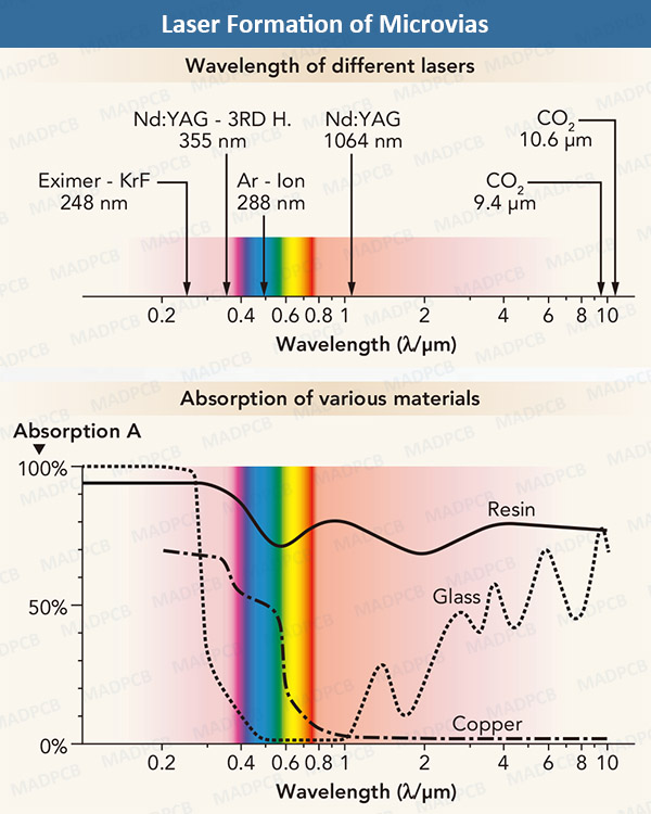
CO2 Laser
CO2 lasers are emitting infrared (IR) light with a wavelength between 9.4μm to 10.6μm. CO2 lasers are primarily used to drill substrates, including resin epoxy, fiberglass, PP, PI, PET, adhesive and coverlay, due to their inability to cut through copper. CO2 lasers are available with a wide range of output power, providing the necessary margin for fast drill processing in circuit board substrates. The relatively long wavelength limits the minimal focus diameter in a given working field area. The formation of vias with diameters less than 3mil (0.075mm) reaches the physical limits of this technology.
UV Laser
The other type of laser used for microvia formation is a solid-state laser emitting ultraviolet (UV) light, generally Nd-YAG. Looking at the absorption spectra copper, epoxy, polyimide and glass it shows that UV light with a wavelength of 355nm (0.355μm) will be absorbed from all those materials. In addition, UV light will be emitted with very short high-power pulses. Precisely focused to a small spot the extreme high-power density creates very concentrated plasma that allows pinpoint ablation of the material.
UV Laser technology creates a number of significant advantages for the drilling for printed circuit boards.
- Both copper and substrate (also including coverlay, EMI shielding film) can be drilled with the same using only one piece of equipment without the need of photochemical etching of the outer copper layer.
- UV lasers are capable of removing the copper layer to expose the fiducials for proper alignment between drill pattern and artwork of the inner layers.
- Microvias with superior quality, large and clean bottoms that are textured and won’t require desmearing.
- The energy exposure in a very small spot for a very short time limits heat spread-out to the drill hole’s environment. This also reduces the danger of delamination of mushroom shaped holes.
- UV lasers allow production of “stacked vias” that connect three layers of the board with one another.
Other benefits of UV laser formation of microvias are:
- The excellent alignment to the inner layer circuitry by using fiducials on the inner layer allows the use of smaller land pads.
- The capability to form stacked vias, connecting three layers reduces the SBU steps.