Table of Contents
Signal Integrity (SI) Services
With the development of electronics technology, more and more designs employ high-speed board connections. Sometimes they are USB2.0, sometimes they are PCI Express, sometimes they are interfaces to DRAM, and so on. These innovations offer huge advantages to the designer and to the customer; however, their high-speed signaling must be respected and the design rules carefully followed.
High Speed Connectivity
High speed interconnects are very sensitive to several manufacturing parameters that can make or break your product. Among those are:
- Reflections in interconnects
- Signal losses within the laminate
- Electromagnetic radiation from the traces
- Quality of ground
A specification of a high-speed connectivity standard, like PCI Express, spends tens of pages discussing these rules, and many standards define very detailed requirements for the entire design. If these requirements are not met the connection will be unreliable or completely unusable because the signals will be too distorted or too attenuated when they reach the receiver. Signal integrity analysis determines how much the signals will be distorted and whether that level of distortion is acceptable for a given connection. This is done my means of computer simulation, before the PCB board is manufactured.
How to Achieve Signal Integrity?
Signal Integrity should be considered by the designer from the moment he starts drawing the schematic and until the moment his board passes the final test. For example, the designer must be aware of trace length restriction or of proper selection of connectors.
Once the schematic is done, the PCB layout is then performed using numerous constraints placed on some nets; these constraints typically are derived from the standard on that particular connectivity. For example, USB2.0 standard tells the designer that the traces should have differential impedance of 90ohm. To achieve that, the layout designer selects a suitable stack-up (they are offered by PCB manufacturers) and then sets up rules that define what traces may go on what layer, and what their geometry should be, and so on.
Once the layout is done, it is a very good idea to verify, by means of computer simulation, that the board meets the requirements of the standard. Many standards offer no help in dealing with interfering signals, breaks in the ground plane, or other complications of a practical PCB board. So, it may be necessary to simulate the routed board to check that the critical high-speed traces are compliant with the standard. This simulation is called Signal Integrity Analysis.
How A PCB Affects High Speed Signals?
We will illustrate typical signal integrity problems on a simple example. Let’s make two differential traces, one that is properly routed and matched, and another that is not of controlled impedance at all. Then we’ll see what happens. The schematic of the example is as following:
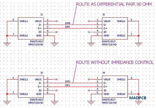
Signal Integrity
The routed PCB for this example:
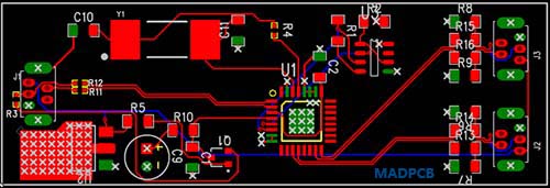
Signal Integrity
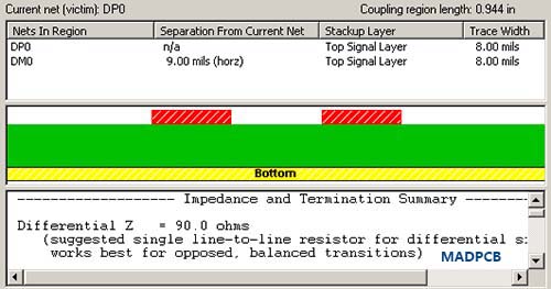
For this example, we choose 90ohm differential pairs, and only one of them is correctly made. This design requires 8mil trace and 9mil space, and the microstrip layout with thickness of laminate slightly less than 5mil. Below is the cross-section of the “good” differential pair:
Signal Integrity
The “bad” connection, to be compared to the “good” one, is routed with traces of wrong width; the separation of those traces is not what it should be, and it varies too.
With these traces prepared, we will now apply test signals to connectors J1 and J3, and will terminate J2 and J4 with 90ohm resistors. We will also connect the differential probe of the oscilloscope to J2 and J4. All this can be simulated in software.
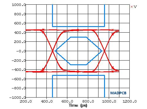
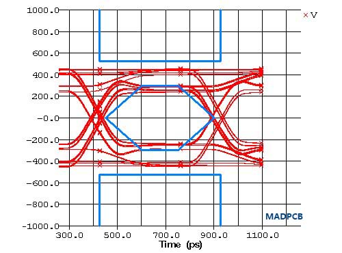
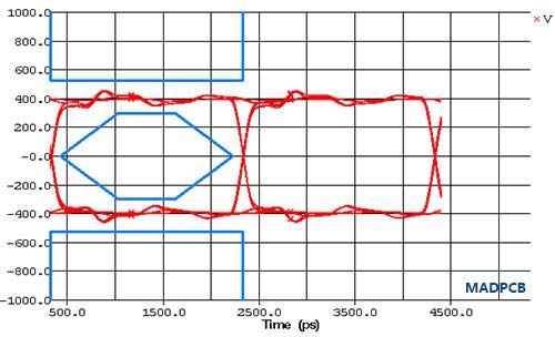
The stimulus that we use is a nearly ideal driver, with 10.980/100.000ps rise and fall time, and the amplitude is 0.5V. The pair is fed with two such drivers, phase of one shifted 180° from another. We choose the data rate to be 2Gbps (the bit interval is 0.5ns.) Below is the eye diagram of the “good” connection:
Signal Integrity
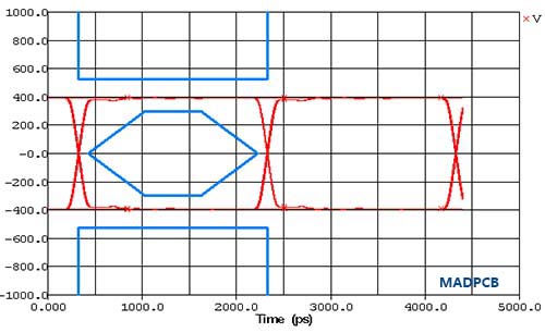
This eye diagram represents an excellent signal integrity. Now let’s move the probes of the oscilloscope to the other, poorly designed, connection and repeat the simulation:
Signal Integrity
This eye diagram is completely unacceptable -the signal enters prohibited areas of the mask. This happens because the impedance of the “bad” pair is not right for the termination, and we can’t change the termination because it is defined by the external equipment.
Design PCB with Signal Integrity in Mind
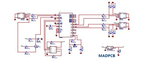
Now we will demonstrate on a simple example how high-speed PCBs may be designed. The schematic below implements a small two-port USB hub; we omitted power switching for clarity.
Signal Integrity
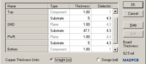
In the next step of the design process, the PCB stack-up is selected. For this sample board, we choose an inexpensive 4-layer construction, with inner layers allocated for planes and outer layers usable for impedance controlled traces.
Signal Integrity
Now the designer can calculate proper trace widths and distances between traces for differential pairs. For this design we will aim for 90ohm differential impedance. A trace width calculator tells us that for our stack-up we should use trace width 8mil and separation of 6.2mil, that will result in impedance that is very close to 90ohm.
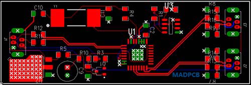
With these decisions made, the printed circuit board designer performs parts placement and routes the board. Below is the PCB routed for this exercise. High speed differential pairs are clearly seen on the top layer.
Signal Integrity
If the Signal Integrity Analysis is not required, the board at this point would be ready to go to fabrication. To perform the Signal Integrity Analysis, the board is transferred into a specialized CAD software that can do simulation of routed traces, vias, and of coupling effects of neighboring traces.
Signal Integrity Analysis Workflow
Step number one is to import the routed PCB into the software. It is then displayed on the screen. Note that only those traces are highlighted that (a) are selected and (b) that are sufficiently close to selected traces to warrant simulation. We can select different traces for simulation, but for this exercise we will focus only on the highlighted differential pair.
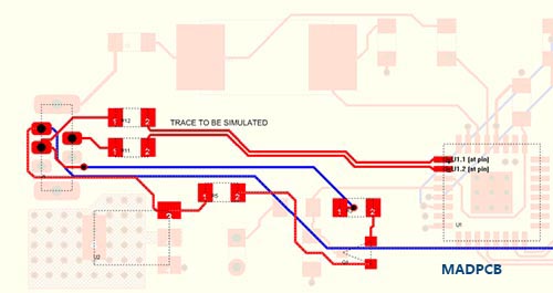
Signal Integrity
The stack-up information is also transferred, and we can review it. Note that the software independently calculated impedances of traces and we can see that our original design decisions were correct:
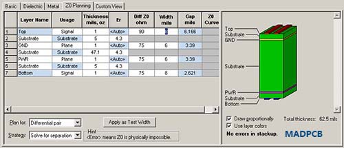
Signal Integrity
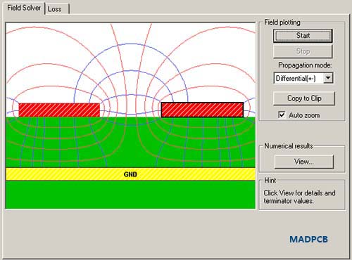
Immediately we are able to select any trace segment and verify the EM field around it. If we select a differential trace then coupling effects will be also calculated. Below is a plot of EM field around the input USB2.0 differential pair:
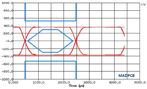
Now we are ready to simulate the high-speed connection from J1 to U1. We attach an ideal driver to the pins of the J1, then we attach a 90ohm terminator at input pins of U1, and we connect the oscilloscope probes to U1. Then we configure the measurement to be eye diagram, with USB2.0 TX compliance mask (as being more strict compared to RX mask,) and we select 2.0ns as the bit period (USB2.0 actually uses 2.083ns bit period.) Below is the result:
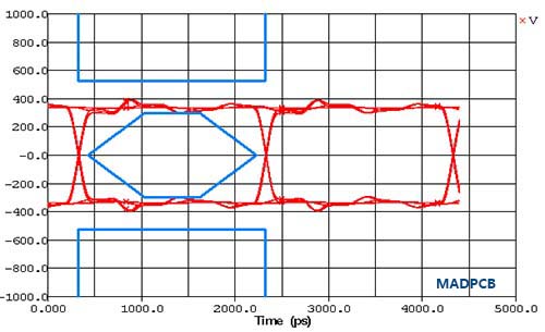
What do we see? We see a marginal performance; traces of the eye diagram touch the mask. Will it work? Probably yes, in controlled environment and with zero tolerance on all parts. Will you want to ship this? Most definitely not. The board, as it appears, has issues -and we wouldn’t know about them without simulation. If there are 100K boards on order already, the designer would be in serious trouble.
What can be done about this? There are two possibilities. We can tweak values of some components on the board, and we can redo the board. The former option is appealing if boards are already fabricated. The latter option is preferred if nothing had been ordered yet.
Let’s start with component tweaking and see how much it buys us. The serial termination resistors R11 and R12 are currently 18ohm, and we see that signal level is too low. We have to live with the ripple (since we are stuck with board,) but we need to raise the level a bit. We can do that by reducing these resistors to, say, 8.2ohm:
It is better now; we managed to center the ripple within the allowed zone of the mask. Now the trace is compliant, and we have some margin. This is the solution if you must use the boards as they are.
A better solution is to fix the board, though. The ripple would be reduced, greatly improving immunity to the noise and to the drift of components’ parameters. Below we make any changes, we need to look closely at the board and understand what is actually wrong with it.
There are following issues with this particular trace:
- The resistors R11 and R12 have large pads; this is because the resistors themselves, 1206, are large. But these pads create impedance bumps. We must use physically smaller components here, with pads that are not much wider than 8 mil. Perhaps 0402 would be adequate; we don’t want to deal with smaller parts.
- The traces between the pins of J1 and R11, R12 are not impedance controlled. Yes, they are short, but we do have problems, and we need to clean up all the defects if we want to get a properly designed circuit.
- There is a long stub hanging off of the J1.3 pin and going to R3. This stub should be very short, and it would also help if R3 is also physically small.
We implemented these changes, and the new PCB is shown below:
Here are results of he simulation done on the improved board:
As we can see, the signal is now nearly flawless, just as we’d like it to be. This simulation indicates that this particular differential trace is now done right.
Finally, the developer may want to look for an IBIS model of a particular component and plug it into the simulation. IBIS models are created by measuring signals that the IC produces and responds to. Large tables of these measurements then are grouped into one file. It is expensive for an IC manufacturer to create and maintain models; because of that not all ICs have models, and not all models are usable.
For this example, we want to drive the pins of J1 with a real USB source, and we picked Cypress Semiconductor CY7C65640 USB 2.0 Hub for that simulation. We changed the model that drives J1.2 and J1.3 and ran the eye diagram again. The results are shown below:
The simulation shows perfect matching. The ripple completely disappeared because the driver within the CY7C65640 is twice as slow as the one we used before, but it is the optimal match to the requirements of the USB2.0 standard. The signal level is also within the mask for the USB2.0 transmitter. We can declare that this trace on our example board is now perfect.
Design of high-speed interfaces is sometimes complicated, and many analog parameters need to be taken into account by the PCB design engineer. Mistakes in the design can be expensive. A Signal Integrity Analysis, done before the PCB boards are sent to manufacturing, can help in detection of those mistakes. Modern software allows to simulate boards and detect problems that otherwise may remain undetected until there is no time left in the project to make changes.