What is Noise in Electronics?
Noise (electronics) is an unwanted disturbance in an electrical signal. Noise generated by electronic devices varies greatly as it is produced by several different effects.
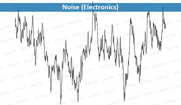
Noise (Electronics)
In communication systems, noise is an error or undesired random disturbance of a useful information signal. The noise is a summation of unwanted or disturbing energy from natural and sometimes man-made sources. Noise is, however, typically distinguished from interference, for example in the signal-to-noise ratio (SNR), signal-to-interference ratio (SIR) and signal-to-noise plus interference ratio (SNIR) measures. Noise is also typically distinguished from distortion, which is an unwanted systematic alteration of the signal waveform by the communication equipment, for example in signal-to-noise and distortion ratio (SINAD) and total harmonic distortion plus noise (THD+N) measures.
While noise is generally unwanted, it can serve a useful purpose in some applications, such as random number generation or dither.
Noise Types
Different types of noise are generated by different devices and different processes. Thermal noise is unavoidable at non-zero temperature (see fluctuation-dissipation theorem), while other types depend mostly on device type (such as shot noise, which needs a steep potential barrier) or manufacturing quality and semiconductor defects, such as conductance fluctuations, including 1/f noise.
- Thermal noise: Johnson–Nyquist noise (more often thermal noise) is unavoidable, and generated by the random thermal motion of charge carriers (usually electrons), inside an electrical conductor, which happens regardless of any applied voltage. Thermal noise is approximately white, meaning that its power spectral density is nearly equal throughout the frequency spectrum. The amplitude of the signal has very nearly a Gaussian probability density function. A communication system affected by thermal noise is often modelled as an additive white Gaussian noise (AWGN) channel.
- Shot noise: Shot noise in electronic devices results from unavoidable random statistical fluctuations of the electric current when the charge carriers (such as electrons) traverse a gap. If electrons flow across a barrier, then they have discrete arrival times. Those discrete arrivals exhibit shot noise. Typically, the barrier in a diode is used.
- Partition noise: Where current divides between two (or more) paths, noise occurs as a result of random fluctuations that occur during this division. For this reason, a transistor will have more noise than the combined shot noise from its two PN junctions.
- Flicker noise: Also known as 1/f noise, is a signal or process with a frequency spectrum that falls off steadily into the higher frequencies, with a pink spectrum. It occurs in almost all electronic devices and results from a variety of effects.
- Burst noise: It consists of sudden step-like transitions between two or more discrete voltage or current levels, as high as several hundred microvolts, at random and unpredictable times. Each shift in offset voltage or current lasts for several milliseconds to seconds. It is also known a popcorn noise for the popping or crackling sounds it produces in audio circuits.
- Transit-time noise: If the time taken by the electrons to travel from emitter to collector in a transistor becomes comparable to the period of the signal being amplified, that is, at frequencies above VHF and beyond, the transit-time effect takes place, and the noise input impedance of the transistor decreases. From the frequency at which this effect becomes significant, it increases with frequency and quickly dominates other sources of noise.
Coupled Noise
While noise may be generated in the electronic circuit itself, additional noise energy can be coupled into a circuit from the external environment, by inductive coupling or capacitive coupling, or through the antenna of a radio receiver.
- Intermodulation noise: Caused when signals of different frequencies share the same non-linear medium.
- Crosstalk: Phenomenon in which a signal transmitted in one circuit or channel of a transmission system creates undesired interference onto a signal in another channel.
- Interference: Modification or disruption of a signal travelling along a medium.
- Atmospheric noise: Also called static noise, it is caused by lightning discharges in thunderstorms and other electrical disturbances occurring in nature, such as corona discharge.
- Industrial noise: Sources such as automobiles, aircraft, ignition electric motors and switching gear, high voltage wires and fluorescent lamps cause industrial noise. These noises are produced by the discharge present in all these operations.
- Solar noise: Noise that originates from the Sun is called solar noise. Under normal conditions, there is approximately constant radiation from the Sun due to its high temperature, but solar storms can cause a variety of electrical disturbances. The intensity of solar noise varies over time in a solar cycle.
- Cosmic noise: Distant stars generate noise called cosmic noise. While these stars are too far away to individually affect terrestrial communications systems, their large number leads to appreciable collective effects. Cosmic noise has been observed in a range from 8 MHz to 1.43 GHz, the latter frequency corresponding to the 21-cm hydrogen line. Apart from man-made noise, it is the strongest component over the range of about 20 to 120MHz. Little cosmic noise below 20MHz penetrates the ionosphere, while its eventual disappearance at frequencies in excess of 1.5 GHz is probably governed by the mechanisms generating it and its absorption by hydrogen in interstellar space.
How to Reduce Noise?
In many cases noise found on a signal in a circuit is unwanted. There are many different noise reduction techniques that can reduce the noise picked up by a circuit.
- Faraday cage – A Faraday cage enclosing a circuit can be used to isolate the circuit from external noise sources. A faraday cage cannot address noise sources that originate in the circuit itself or those carried in on its inputs, including the power supply.
- Capacitive coupling – Capacitive coupling allows an AC signal from one part of the circuit to be picked up in another part through the interaction of electric fields. Where coupling is unintended, the effects can be addressed through improved circuit layout and grounding.
- Ground loops – When grounding a circuit, it is important to avoid ground loops. Ground loops occur when there is a voltage difference between two ground connections. A good way to fix this is to bring all the ground wires to the same potential in a ground bus.
- Shielding cables – A shielded cable can be thought of as a Faraday cage for wiring and can protect the wires from unwanted noise in a sensitive circuit. The shield must be grounded to be effective. Grounding the shield at only one end can avoid a ground loop on the shield.
- Twisted pair wiring – Twisting wires in a circuit will reduce electromagnetic noise. Twisting the wires decreases the loop size in which a magnetic field can run through to produce a current between the wires. Small loops may exist between wires twisted together, but the magnetic field going through these loops induces a current flowing in opposite directions in alternate loops on each wire and so there is no net noise current.
- Notch filters – Notch filters or band-rejection filters are useful for eliminating a specific noise frequency. For example, power lines within a building run at 50 or 60 Hz line frequency. A sensitive circuit will pick up this frequency as noise. A notch filter tuned to the line frequency can remove the noise.
Thermal noise can be reduced by cooling of circuits – this is typically only employed in high accuracy high value applications such as radio telescopes.
Qualification
The noise level in an electronic system is typically measured as an electrical power N in watts or dBm, a root mean square (RMS) voltage (identical to the noise standard deviation) in volts, dBμV or a mean squared error (MSE) in volts squared. Examples of electrical noise-level measurement units are dBu, dBm0, dBrn, dBrnC, and dBrn(f1 − f2), dBrn(144-line). Noise may also be characterized by its probability distribution and noise spectral density N0(f) in watts per hertz.
A noise signal is typically considered as a linear addition to a useful information signal. Typical signal quality measures involving noise are signal-to-noise ratio (SNR or S/N), signal-to-quantization noise ratio (SQNR) in analog-to-digital conversion and compression, peak signal-to-noise ratio (PSNR) in image and video coding and noise figure in cascaded amplifiers. In a carrier-modulated passband analogue communication system, a certain carrier-to-noise ratio (CNR) at the radio receiver input would result in a certain signal-to-noise ratio in the detected message signal. In a digital communications system, a certain Eb/N0 (normalized signal-to-noise ratio) would result in a certain bit error rate. Telecommunication systems strive to increase the ratio of signal level to noise level in order to effectively transfer data. Noise in telecommunication systems is a product of both internal and external sources to the system.
Noise is a random process, characterized by stochastic properties such as its variance, distribution, and spectral density. The spectral distribution of noise can vary with frequency, so its power density is measured in watts per hertz (W/Hz). Since the power in a resistive element is proportional to the square of the voltage across it, noise voltage (density) can be described by taking the square root of the noise power density, resulting in volts per root hertz. Integrated circuit devices, such as operational amplifiers commonly quote equivalent input noise level in these terms (at room temperature).
Dither
If the noise source is correlated with the signal, such as in the case of quantization error, the intentional introduction of additional noise, called dither, can reduce overall noise in the bandwidth of interest. This technique allows retrieval of signals below the nominal detection threshold of an instrument. This is an example of stochastic resonance.
Possible Sources of Noise in PCB
In a printed circuit board, noise is typically produced by current spikes that occur on some electrical signals. In digital circuits, current spikes are created during transistor switching (on-off and off-on transitions), while in analog circuits they are determined by changes in the load current. Frequently, excessive noise can also be due to a floating ground or to an incorrect ground connection. If the maximum frequency of the signals on the PCB is less than 1 MHz, a single ground point is generally sufficient, while for high frequency circuits, a multipoint or star ground connection is preferable. There is also the hybrid configuration, which uses both a single point for low frequency and a multipoint for high frequencies.
The main noise sources can be classified as follows:
- Ground bounce: in digital circuits, the fast and relentless rise of switching frequencies means that electrical signals have less and less time to return to the ground reference level. This can cause the signal to “bounce” above ground level, generating unexpected current spikes and resulting in noise in the output signal. In the case of multiple simultaneous switching, the amount of noise can also produce false or double switching, resulting in a malfunction of the circuit
- Crosstalk: if the PCB traces are not sufficiently spaced apart, it may happen that a signal (high frequency or high current) influences the behavior of a signal that travels an adjacent trace. This phenomenon of undesired electromagnetic coupling is called crosstalk and can occur both when the traces are too close to each other horizontally on the same layer, and vertically on adjacent layers
- EMI (Electro Magnetic Interference): electromagnetic interference can be produced by numerous sources, although the most common case concerns incorrectly designed ground return paths. The general rule to avoid these phenomena is to insert the traces of the signals between the power and ground planes, allowing a smooth return path towards the ground plane. When this is not done, the return signal will follow irregular paths trying to find its way to ground, generating interference and noise.