What’s EMI?
Electromagnetic Interface (EMI) is electromagnetic energy that disturbs the signaling in an electronic device through radiation, electrostatic coupling or induction. The disturbance may degrade the performance of the circuit or even stop it from functioning. In the case of a data path, these effects can range from an increase in error rate to a total loss of the data. From the static on your radio to that buzz you hear when you bring a mobile phone near audio device, EMI is all around us.
In PCB design, high-frequency signal transmission always requires EMI shielding for prevent signal loss. In PCB manufacturing, commonly seen in flex and rigid-flex board, an EMI shielding film, carbon paste or silver paste is applied onto the PCB surface. In PCB assembly, we always require assembling a stainless steel EMI shielding cover onto the some areas.
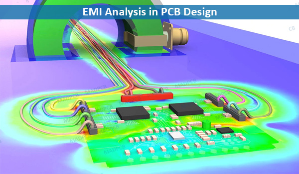
EMI Analysis in PCB Design
What are the Sources of EMI?
There are two types of electromagnetic emission: conducted and radiated emission. Conducted emission enters the system through power input lines and cables. While, the radiated emission happens due to electromagnetic waves from power and communication lines, switching devices, and electrostatic discharges. It propagates through the air from electronic devices and traces, to interfere with other electronic systems. Examples are mobile and laptops interfering with aircraft electronics. Conducted interference can be mitigated by introducing line filters connected close to the power input or near the connectors. Another effective method for reducing conducted interference is using a ferrite core/ferrite ring. Ferrite core employs high-frequency current dissipation in a ferrite ceramic to build high-frequency noise suppression devices.
Electromagnetic emissions may also occur from high-frequency traces. Similarly, they can generate from power and ground planes, due to poor decoupling practices. This also results in unintentional currents, such as common-mode (CM) and differential-mode (DM) currents.
Faraday’s law states that the magnetic field generated by a coil is directly proportional to the area of the coil and the current.
E = di/dt ∝ Coil Area ∝ Current going through the coil
- Reducing the coil/loop area. When this loop area decreases, the magnetic flux will also reduce. Now, the question is, how we can do it? Let’s say, we have a trace on the top PCB layer, we can reduce the loop by placing a ground plane directly under the trace/signal. So, when do this, the current goes through the trace following the device and returns through the ground plane. The thickness of the PCB is around 3mils, and thus the area becomes very small. This is low how placing the ground plane exactly below the trace reduces EMI because it reduces the overall area to be traversed.
- Minimizing the rate of change of current. The higher current causes more emissions. So, if you reduce the current, EMI can also be reduced. Maintaining low rise times, even if your PCB is operating at high-frequency, can also be helpful for EMI reduction.
- Avoiding impedance mismatching: A properly designed circuit board or system always comes with matched impedance from the source, to the transmission line, and the load. It provides maximum power transfer and minimizes reflections. Reflections on the transmission line increase harmonics, which increases radiated emissions. Unmatched impedances cause ringing and overshoot in digital signals, resulting in more radiated emissions. Properly matched impedances are required because they reduce the radiated emissions from the device.
PCB Design Guidelines for EMI and EMC Reduction
How to design a board with low or absolutely zero electromagnetic interference (EMI)? Well, it is possible. The below design practices will make sure you do not create antennas, which will emit electromagnetic energy. These best design practices will reduce the length and area of the potential signal returns that may increase unwanted EM emissions. The multilayer PCB stack-up will play a critical role, particularly in high-power and digital applications. Signal traces from components to the processor should be properly routed to avoid any return path, which could lead to common-mode signal generation.
The use of surface-mount devices (SMDs) instead of leaded devices will further reduce EMI/EMC issues. SMDs offer lower inductances in comparison with RF energy. Additionally, SMDs offer higher density due to closer component placements. This is particularly critical in a two-layer or four-layer circuit boards. However, the rising complexity in the PCB design will create more problems associated with line spacing or trace spacing. The dense physical dimensions of SMDs will offer more effective noise-control.
Leaded components with higher inductances will generate a resonant frequency of more than 100MHz. Therefore, the adoption of a large number of through-hole components is not recommended as they generate excessive noise. There are no hard and fast rules for PCB design. Some design rules apply to a certain type of board but not feasible for other types. Nonetheless, at MADPCB, we have curated some general PCB design rules, common to all board types.
Trace Spacing and Layout
- Trace Separation: All signals (clocks, video, audio, reset, ect.) must be separated from other traces. The general rule says that separation between the traces should be 3W, where W is the width of the trace. This practice helps to reduce crosstalk and coupling between adjacent traces on the same PCB layer. Differential traces are an exception to this rule.
- Avoid right-angle and adopt 45° turn: When a trace encounters a 90° bend, the capacitance increases, resulting in the change of characteristic impedance value, which leads to reflections. It can be avoided by replacing sharp bends with 45°
- Route differential traces closely: It increases the coupling factor and keeps the noise in common mode. For example, let us assume two wires, which are placed close to each other. Any external noise intervening with these two traces will add the same amount of disturbance in both the traces. If trace 1 has 1V and trace 2 has 1.5V, then the difference would be 0.5V. Since, the external noise will actually cancel out. That is why high-speed signals are preferably routed as differential pairs.
- Use vias like a pro: Vias are used in multilayer PCBs for signal routing purposes. A good designer must know that each via comes with its capacitance and inductance effect. So, vias should be avoided as far as possible and critical traces should be routed on the same layer. Because of the parasitic capacitance and inductance in the vias, there is an impedance mismatch between via and trace, which creates reflections. When vias cannot be avoided, it should be ensured that ground vias should be placed close to the signal vias. This will ensure that the signals are referenced to connected grounds and this reduces the change in the characteristic impedance value and thus reflections. In differential pairs, when vias cannot be avoided, the same number of vias should be put in both traces. Avoid vias in differential traces. If you have to then use anti-pad shared by two vias to minimize parasitic capacitance.
- Avoid stubs in sensitive and high-frequency traces: Stubs produce reflections as well as the potential of adding fractional wavelength antenna to the circuit.
- Use guard and shunt traces for clock lines: In clock circuits, decoupling capacitors are very important for supposing noise propagating along the supply rails. Guard and shunt trace are used to protect clock lines from EMI sources, otherwise, such clock signals will create problems elsewhere in the circuit.
Ground Planes
A ground with low inductance value is a crucial element during PCB design for mitigating EMC problems. Increasing the ground area on a PCB reduces the ground inductance in the system, hence EM emission and crosstalk too. Several approaches are available when we need to connect the signals to the ground, but what is best? Before jumping to the best PCB design approach, let us discuss what is not at all acceptable? Never connect the PCB components randomly to the ground points. So, what is the recommended design approach?
- Use full ground plane and ground grids: Use the entire ground plane since it offers the least inductance value when the signal returns to the source from the load. Although a ground requires a dedicated PCB layer, this may not always be possible in a two-layer PCB. PCB designers use ground grids, where the inductance of a ground grid depends upon the distance between the grids.
- Avoid long return paths: As per Faraday’s law, how a signal returns through the system ground makes all the difference. When a signal takes a longer path, it creates a ground loop that forms a radiating antenna. A short return path has a lower impedance, which gives better EMC performance. Long return paths are responsible for greater mutual coupling resulting in crosstalk. Therefore, keep the return paths as short as possible and the loop area as small as possible. The current return path should be handled precisely. It is recommended to connect the device grounds directly to the ground plane. This will reduce the ground loops.
- Use Faraday’s cage/guard ring to isolate the noisily environment: A Faraday cage is created by adding the ground on the edge of the PCB. The purpose is not to route any signal outside this boundary. This technique restricts the emission/interference within the defined limit.
- Always ground the copper fill areas: Floating copper traces should always be grounded. Otherwise, it may act as an antenna, causing EMC issues.
- Check for multi-power requirements: When a circuit requires more than one power supply, then it is the best idea to keep them separated by a ground plane. But multi-ground planes cannot be realized in single-layer PCBs. This problem can be solved by running power and ground tracks for one supply separated from the others. It will also avoid noise coupling from one power source to the other.
- Be careful with split apertures: Split apertures that are long holes and wide vias in power and ground planes create a non-uniform area. This non-uniformity increases the impedance in power and ground planes.
Shielding
Shielding is mechanical technique that uses conductive/magnetic (or both) materials to prevent EMI in the system. A mechanical shield is a closed conductive container connected to the ground, which effectively reduces the size of loop antennas by absorbing and reflecting a part of their radiation. It can be used either to cover the whole system or a part of it, based upon the requirement. EMI/EMC shielding protects the signal transmission from external noise and prevents information loss.
Arrangement of PCB Layers
EMC performance of a PCB also depends upon the arrangement of its layers. In the case of two or more than a two-layer board, one entire layer should be used as a ground plane. For a 4-layer board, the layer below the ground layer should be used as a power plane. The preferred layer stack for a 4-layer board is signal 1, ground, power, and signal 2. The impedance-matched traces should be on signal 1 as far as possible.
- If a two-layer board is used and an entire layer of ground is not possible, then ground grids should be used.
- If a separate power plane is not used, then ground traces should run in parallel with power traces to keep the supply clean.
- When there are more than four layers, it is recommended to use PCB layers’ arrangement like signal layer – ground/power layer – signal layer – ground/power layer – signal layer – ground/power layer -signal layer. That is to use alternate signal and ground layers. And, the number of layers should be even.
Segregate Sensitive Components
For an EMC-friendly design, PCB components need to be grouped according to the signals they are operating on, such as analog, digital, power supply, low-speed, high-speed signals, etc. The signal tracks for each component ground should stay in their defined area. It is good to use a filter, whenever a signal has to flow from one subsystem to another.
Decoupling Capacitor
When ICs are operating, they switch current at high-frequency, which results in switching noise in the power rails/traces connected to the IC. This noise if not controlled, will result in radiated emissions and thus EMI. The methods to reduce power rail noise is to place the decoupling capacitors close to the IC power pins. And, grounding the capacitors directly to the ground planes. The use of power planes instead of power traces will also reduce power noise.
Controlled Impedance for Transmission Line Design
When a circuit operates at a high-speed, the impedance matching between the source and destination becomes critical. If the impedance is not matched and controlled properly then it will cause signal reflection and high-frequency ringing. The excess RF energy generated due to ringing and reflection, will radiate/couple to other parts of the circuit, creating EMI problems. Signal termination strategies help to reduce these undesirable effects. Termination not only mitigates signal reflection and ringing by controlled impedance measures but can also slow down the fast-rising and falling edges of the signals. The impedance of traces also depends on the PCB materials used on the board.
Testing EMI/EMC in a PCB Design
The electromagnetic emission in an electronic system is measured by implementing various modeling techniques. The computer simulation is often regarded as the fundamental approach in EMC analysis. The computer simulation is performed via an integration technique to get an accurate measurement of essential parameters. Several steps are followed to test electromagnetic emission in an electronic system:
- The finite difference time domain modeling is implemented to measure the frequency response of the common-mode current during the high voltage applications.
- The common-mode current is evaluated by considering factors such as current-mode antenna impedance, and the distributed circuit constant.
- The electronic coupling between the power plane and the ground plane will also impact the common-mode current.
MADPCB measures the frequency response of electromagnetic emission from the stripline structure with the help of a high-end tool and our own proposed model. We understand the importance of keeping EMI out, thus, we offer physical insights and design guidelines to keep your circuit safe and sound.
Meeting EMI/EMC Standards (CICPR, FCC Section 15)
The objective of EMC/EMI standards is to maintain compatibility between the co-located electrical and electronic system for trouble-free operation. CISPR standards are applicable to all products, systems, and installations. They are introduced following the Federal Communications Commission (FCC) Section 15, and the European International Special Committee on Radio Interference (CISPR) regulations.
The standards define permissible limits for both conduced and radiated emissions and their classification into residential, commercial, light industrial, and industrial environments. To meet EMC requirements, the device must be tested for conducted and radiated emissions along with conducted and radiated susceptibility.