What Is a PCB Transmission Line?
A PCB Transmission Line is a type of interconnection used for moving signals from their transmitters to their receivers on a printed circuit board (PCB). A PCB transmission line is composed of two copper traces: a signal trace and a return path (ground plane). The thickness between the two traces is made up of the PCB dielectric material, like Fiberglass, PP, Polyimide and Coverlay.
PCB Tranmission Lines
All I/O signals in a PCB system travel through transmission lines.
- For single-ended I/O interfaces, both the signal trace and the reference plane are necessary to transmit a signal from one place to another on the PCB.
- For differential I/O interfaces, the transmission line is formed by the combination of two traces and a reference plane.
Impedance Controlled Transmission Lines
The alternating current (AC) that runs on a transmission line usually has a high enough frequency to manifest its wave propagation nature. The key aspect of the wave propagation of the electrical signals over a transmission line is that the line has an impedance at every point along its length and if the line geometry is the same along the length, the line impedance is uniform. We call such a line a controlled impedance line. Non-uniform impedance causes signal reflections and distortion. It means that at high frequencies, transmission lines need to have a controlled impedance to predict the behavior of the signals.
It is crucial to not ignore the transmission line effects in order to avoid signal reflections, crosstalk, electromagnetic noise and other issues which could severely impact the signal quality and cause errors.
While the presence of a reference plane is not strictly necessary in the case of differential signals, it is necessary for practical implementation of differential traces in printed circuit boards (PCBs). Good signal integrity in a PCB system is dependent on having transmission lines with controlled impedance. The impedance is determined by the geometry of the traces and the signal trace and the reference plane.
The dielectric constant (Er or Dk) of the dielectrics varies from board to board, it is fairly constant within one board. Therefore, the relative impedance of transmission lines in a PCB is defined most strongly by the trace geometries and tolerances. Impedance variance can occur based on the presence or absence of glass in a local portion of the lamination weave, but this rarely poses issues except in high-speed (>6GB/s) interfaces.
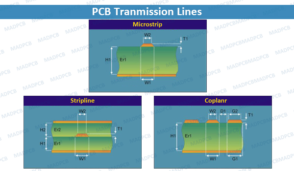
How Many Types of Transmission Line?
In printed circuit boards, there are usually two basic types of signal transmission line, including Microstrip and Stripline. While, there is a third type –Coplanar without a reference plane but it is not very common in PCB design.
- Microstrip: It is composed of a single uniform trace – for the signal – located on the outer layer of a PCB, and parallel to a conducting ground plane, which provides the return path for the signal. The trace and the ground plane are separated by a certain height of PCB dielectric. Below is an uncoated microstrip.
- Stripline: It is composed of a uniform trace – for the signal – located on the inner layer of a PCB. The trace is separated on each side by a parallel PCB dielectric layer and then a conducting plane. So, it has two return paths – reference plane 1 and reference plane 2.
- Coplanar: A coplanar waveguide structure has the signal trace and the return path conductor on the same layer of the PCB. The signal trace is at the center and is surrounded by the two adjacent outer ground planes; it is called “coplanar” because these three flat structures are on the same plane. The PCB dielectric is located underneath. Both microstrips and striplines may have a coplanar structure.