Table of Contents
Plated Half-Holes | Castellated Holes
Plated Half-Holes, also referred to Castellated Holes, are rows of holes are drilled alongside the boundaries of a rigid printed circuit board (PCB), then to be through plated and milled off half. You may have seen some Wi-fi modules which then soldered onto a larger PCB similar to the way in which ICs are mounted. Plated half-holes are mainly used for board-on-board connections, mostly where two PCB boards with different technologies are soldered together.
Economical Board-to-Board Technique
In past, if want to solder a daughter board to a mother board, it requires a board-board connector, which takes much space and increases some project cost. But now if your system can be realized with half-holes technique, you can remove the connector, and make the PCB assembly easy and economical. PCB with plated half-holes on the boundaries stands for the daughter board or surface mount part, will mount flush on the surface of mother board.
Board-to-board PCBs need plated half-holes, which serve as solder mounting device (SMD) terminal pads. Through directly soldering and connecting to the mother PCB, the whole system is considerably thinner than a comparable connection with multi-pin connectors. In one hand, plated-half-hole is an economical connection technique, which can convert the circuit board into surface mounted assembly. In another hand, it can provide a better landing for soldering as it is concave and plated.
How to Design Half-Holes?
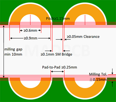
At MADPCB, half-holes PCB manufacturing should follow the capabilities as showed as the figure below.
When layout your PCB, you should keep some guidelines in mind.
- Min feature pitch between two nearby holes is 1.15mm
- Min drill diameter for forming half-holes is 0.6mm
- Min hole pad diameter is 0.9mm
- Min solder mask clearance of half-holes is 0.05mm
- Min solder mask bridge is 0.1mm
- Min Pad-to-Pad distance is 0.25mmm
- Milling tolerance for holes halving is +/-0.15mm
- ENIG is the recommended surface finish, but depends on the application of the board
- Number of the half holes has no limit, but much number of holes makes the PCB assembly easier.
Half-holes can be applied in double-sided and multilayer PCBs. Try to use larger holes than 0.6mm and larger hole pad than 0.9mm as possible as you can. When design plated half-holes on your multilayer PCB, if possible, connect inner layer pads to the plated holes for halving, which brings more stability and helps to avoid burrs.
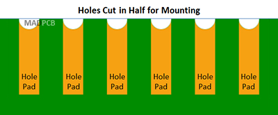
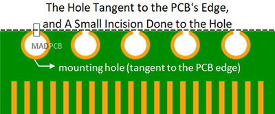
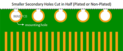
3 Main Designs of Half-holes
How to Define Half-Holes?
Half-holes design varies from CAD software, but the desired result in Gerber files should be as follow. Add rows of plated-thru holes (vias) on the boundaries of the board where the half vias required, and make sure 1/2 circle of the plated holes on the board body and another 1/2 circuit on the outside of the outline.
Besides, the followings should be included in your Gerber files zip folder:
- Outer copper layers: copper pads on both top and bottom copper layers of all half holes.
- Solder mask layers: solder mask openings on both sides.
- Mechanical & Outline layers: the outline should across the holes need to be half routed.
Plated Half-Holes Manufacturing Process
Outer and inner half-holes in prototype and high-volume PCBs are manufacturable at MADPCB, which increases PCB design flexibility without compromising on quality. With our advanced manufacturing process, the yield can be guaranteed. What’s more, no restriction on PCB shape or panel layout, excluding general rules that apply to all PCB designs.
Whole vias for halving are made as standard board on the edge of the boards. A milling toll is then used to cut the plated holes in half. Copper on hole wall is harder than core material (FR4, PTFE), the milling bit will likely go broken. It’s necessary to use heavy duty milling bits when milling the holes at a high speed, which will result in a smoother finish. All half-holes are then inspected in a dedicated station and deburred as our quality control standards.
Applications
- Half-holes can be used as breakout boards for a particular portion of the large PCB.
- These holes give ease to change the Pin layout of the component as per the user requirement.
- Integrated modules can be produced on a single PCB using castellation, which can be used further into assembly during production.
- PCBs with castellated holes can be mounted easily to another PCB during PCB assembly process.
- They are used to combine two boards to validate the solder joint quality.
- They are used for breakout boards or small modules like wifi modules.
- Plated half-hole also help to create wireless PCB to PCB connection.


