Table of Contents
BGA Assembly, Rework & Reballing Services
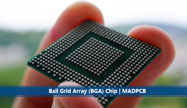
What is BGA?
When it comes to BGA assembly, what’s a BGA? BGAs (Ball Grid Arrays) are IC packages, which place output pins in the form of a solder ball matrix. The traces of the BGA are generally fabricated on laminated substrates (BT-based) or polyimide-based films. Therefore, the entire area of substrates or films can be used to route the interconnection. BGA has the advantage of lower ground or power inductance thereby assigning ground or power nets via a shorter current path to the PCB board.
BGA
Thermally enhanced mechanisms (heat sink, thermal balls, etc.) can be applied to BGA in order to reduce resistance. The greater functional capabilities of the BGA package technology benefit high power and high-speed ICs that require enhanced electrical and thermal performance. Compared with traditional SMT packages, the advantages of BGA are as follows:
- Higher interconnect density
- Lower assembly cost
- Self-alignment during reflow
- Lower profile
- Ease of thermal and electrical management
- Ease of routing
Know-hows of BGA Assembly
Offering short signal paths, controlled line impedance, and a solution for integrated circuits (IC) with high interconnect density, BGA packages provide a means of reducing component size while supporting high-density interconnect requirements with Via-in-Pad technology, which seems to be one of the hottest PCB topics these days, and also a bit of a tough one in PCB assembly. While, how to guarantee BGA assembly quality? How to inspect BGA soldering quality? and how to implement rework on BGAs with soldering defects?
All PCB assembly manufacturers are required to understand and know how to solve them in any SMT assembly project. MADPCB has been providing BGA assembly, with BGA rework and BGA re-balling services in the printed circuit board assembly industry for more than 1 decade, and we totally got the know-hows to build high-quality and high-yield BGA boards for you.
BGA Assembly Capability

BGA Assembly
MADPCB is the reliable turnkey PCB assembly provider you can count on, we have rich experience of handling all types of BGAs, from micro BGA (2mm x 3mm) to large size BGAs (45mm); from ceramic BGAs to plastic BGAs. We are capable of placing minimum 0.25mm pitch BGAs on your board. Supported BGAs are listed as below,
- BGA -Ball Grid Array
- μBGA -Micro BGA
- CABGA -Chip Array BGA
- CTBGA -Thin Chip Array BGA
- CVBGA -Very Thin Chip Array BGA
- DSBGA -Die-size BGA
- FBGA -Fine BGA (also known as Fine Pitch BGA, mainly used for system-on-a-chip design)
- LGA -Land Grid Array
- CSP -Chip Scale Package
- WLCSP -Wafer Level Chip Scale Packaging
- FCBGA -Flip Chip BGA
- FCμBGA -Flip Chip Micro BGA
- LBGA -Low-profile BGA
How to Guarantee BGA Assembly Quality?
PCB Pad and Via Design
BGA assembly quality is vital to the function realization of your design. Before BGA soldering, we need to know BGA packages. Generally, the solder-ball terminal on a BGA package is formed on a Solder-Mask-Defined (SMD) pad. Components with Non-Solder-Mask-Defined pads (NSMD) on the package are also available. Figures below shows the differences between both types.
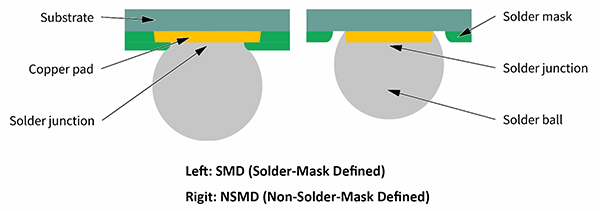
Solder-Mask-Defined (SMD) and Non-Solder-Mask-Defined (NSMD) BGA packages.
The quality and reliability of interconnect solder joints to the PCB board are affected by:
- Pad type (Solder-Mask Defined, SMD or Non-Solder-Mask Defined, NSMD)
- Specific pad dimensions
- Pad surface finish
- Via layout and technology
The NSMD pad type on PCB is preferred since it allows for appropriate pad precision and good board reliability. Please choose a specific package when searching the BGA datasheet, which will then show an example of the stencil aperture layout for each package. Design details will depend on the PCB technology used, the capability of the PCB manufacturers and suppliers, and the planned routing. In most designs, PCB designers always use BGA solder balls with SMD pad design on the component side and with NSMD pad design on the PCB side. Investigations on board-level reliability have shown that in most cases this configuration results in the highest solder-joint reliability. The NSMD pad on the PCB allows the solder to grip the PCB pad sidewalls, improving the reliability of the solder joint.
If any kind of via hole is placed inside the pad area, its opening should be closed by plugging or plating in order to prevent solder flow into it. If closed microvias are placed inside the pads, their intersection with the pad should be flat as possible with Via-in-Pad manufacturing process.
Solder Paste Stencil Design
In BGA assembly, the solder paste is applied onto the PCB metal pads by stencil printing. The volume of the printed solder paste is determined by the stencil aperture and the stencil thickness. The stencil aperture for BGA packages should be circular. The stencil thickness can vary between 100μm (4mil) and 150μm (6mil) depending on aperture area ratio, the stencil material, and the aperture diameter.
To ensure a uniform and sufficient solder paste transfer to the PCB, laser-cut stencils (mostly made from stainless steel) are preferred. For individual design adaptations to use the optimum amount of solder, the stencil thickness, the PCB pad finish, quality and solder masking, the via layout and the solder paste type should be considered. In every case, application-specific experiments are recommended.
Component (including BGA) Placement
Although the self-alignment effect due to the surface tension of the liquid solder will support the formation of reliable solder joints, the BGA components have to be placed accurately depending on their geometry. Positioning the packages manually is not recommended, especially for packages with small terminals and pitch. An automated pick-and-place machine is recommended to obtain reliable solder joints.
Including BGA packages, component placement accuracies of +/-50μm and less are obtained with modern automatic component placement machines using CCD camera. With these systems, both the PCB and the components are optically measured and the components are placed on the PCB at their programmed positions. The fiducials on the PCB are located either on the edge of the PCB for the entire PCB, or at additional individual mounting positions (local fiducials). These fiducials are detected by a vision system immediately prior to the mounting process. Most such vision systems provide special lighting and algorithms for area array packages. For BGA components, it is recommended to use the ball recognition instead of the component outline recognition for centering. This approach eliminates potential tolerances between the solder ball and the package.
When placing BGA packages, the placement force should be sufficiently high, while avoiding excessive placement force that can squeeze the solder paste out of its intended location and cause solder joint shorts.
BGA Reflow Soldering
When the board with BGA packages placed comes to reflow soldering. The soldering profile should be in accordance with the recommendations of the solder paste manufacturer to achieve optimal solder-joint quality. The position and the surrounding of the component on the PCB, as well as the PCB thickness, can influence the solder joint temperature significantly.
BGA packages are generally suited for double-sided PCB mounting. That means that both sides of the PCB are fitted and reflowed one after another. As a consequence, the side that was initially assembled experiences two reflow cycles. During the second cycle, the components are hanging upside-down. Therefore, during the peak reflow zone of the reflow profile (where the solder is liquid), the components are only held by wetting forces of the molten solder. Gravity acting in the opposite direction will elongate the solder joints, unlike joints on the top side, where gravity forces the components nearer to the PCB surface. This shape will be frozen during cooling and therefore will result in a higher stand-off on the bottom side after the reflow process. Any mechanical impacts on components that are soldered upside down should be avoided.
BGA components have a natural tendency for warpage due to its layered construction. During package development projects the warpage is addressed by specific investigations in order to minimize a potential impact on the solder joint formation.
How to Inspect BGA Soldering Quality?
No matter single-sided or double-sided PCB assembly, when reflow soldering complete. We need to inspect the soldering quality including resistors, capacitors, inductors, BGA and etc. placed on the board.
Optical Solder Joint Inspection
A visual inspection of the BGA solder joints with conventional AOI system is not possible. Even a side-view can only reveal a certain number of the terminal solder balls in their area array configuration. For engineering tasks, cross-sectioning can offer detailed information about the solder joint quality. Due to its destructive character, cross-sectioning during monitoring is naturally not practical.
X-ray Solder Joint Inspection
Automated X-ray inspection (AXI) systems are appropriate for efficient inline control of components such as BGA whose terminals cannot be inspected properly by optical systems. AXI usually consist of an X-ray camera and the hardware and software needed for inspection, controlling, analyzing, and data transferring routines. These reliable systems enable the user to detect BGA soldering defects such as poor soldering, bridging, voiding, and missing parts. However, other defects such as broken solder joints are not easily detected by X-ray.
Figure below shows a section of an X-ray photograph of a properly soldered BGA component. Balls and bond wires as well as vias visible. X-ray images might also reveal a certain amount of voiding in the solder balls. The extent of voiding depends on the solder paste, the reflow profile, and the presence of microvias-in-pad.

X-ray Inspection for Assembled BGA Chip
For the acceptability of electronics assemblies, please refer also to the IPC-A-610 standard [6].
How to Implement BGA with Soldering Defects?
Single solder joint repair of bottom-only terminated packages is highly difficult, if not impossible, and is therefore generally not recommended. Furthermore, the reuse of de-soldered components is not recommended. The de-soldered components should be replaced by new ones. But it’s dependable. At MADPCB, we also can rework most BGA components with soldering defects by re-balling.
A rework process is commonly done on special rework equipment. There are various systems available that meet the requirements for reworking SMD packages. All handling guidelines in this page have to be respected. Special focus should be on the following items:
Due to the decreased automation level given by the general rework approach, even higher care compared to standard PCB assembly must be taken. Tools that do not damage the component mechanically have to be chosen. Mechanical forces that do not necessarily causes visible external damage can still cause internal damage that reduces the BGA’s reliability. A proper handling system with vacuum nozzle may be the gentles process and is therefore recommended. However, the impact of BGA rework tools has to be assessed properly. In general, more manual handling increases the effort for documentation, training, and monitoring of the rework process(es).
During BGA rework, special care must be taken concerning the proper moisture level of the component according to the J-STD-033. Drying the PCB and the component prior to rework might be necessary. A proper drying procedure for SMD packages is described in J-STD-033 standard [3]. Please also refer to the recommendations of PCB assembly manufacturer and take all specific needs of components, PCB, and other materials into account.
Whatever heating system is used (hot air, infrared, hot plate, etc.), the applied temperature profile at the component must never exceed the maximum temperature according to the J-STD-020 standard. Depending on the specific heating profile used during rework, components adjacent to the mounting location might also experience a further “reflow run” in terms of the J-STD-020 standard [2]. Internal investigations have shown that the temperature profile must be recorded.