What Is the IC Package?
Integrated Circuit (IC) Packaging refers to the material that contains a semiconductor device. The IC package is a case that surrounds the circuit material to protect it from corrosion or physical damage and allow mounting of the electrical contacts connecting it to the printed circuit boards (PCBs). There are many different types of integrated circuits, and therefor there are different types of IC packaging systems designs to consider, as different types of circuit designs will have different needs when it comes to their outer shell. IC packages are classified as indicated according to shape, material and mounting methods, you can refer to following figure IC Packages.
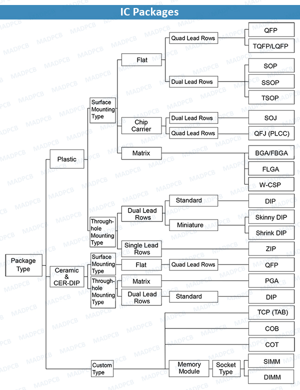
IC Packages
What Is IC Packaging?
IC Packaging is the last stage in the production of semiconductor devices. During this stage, the semiconductor block gets covered in a package that protects the IC from potentially damaging external elements and the corrosive effects of age. The package is essentially an encasement designed to protect the block and also to promote the electrical contacts that deliver signals to the printed circuit board (PCB) of an electronic device.
IC Packaging technology has evolved since the 1970s when ball grid array (BGA) packages first came into use among electronics packaging manufacturers. At the dawn of the 21st century, newer options in package technologies eclipsed pin grid array packages, namely the plastic quad pack and the thin small outline package. As the noughties progressed, manufacturers like Intel ushered in the era of land grid array packages.
Meanwhile, flip-chip ball grid arrays (FCBGAs), which accommodate more pin counts than other package types, superseded BGAs. The FCBGA contains input and output signals over the whole die, as opposed to just the edges.
What Are the Names of IC Packages?
Beyond the basic structural definition of an IC package, further categories distinguish secondary types of interconnection. Further information about the different categories of IC packages can be found below:
- Pin-Grid Array: These are for socketing.
- Lead-frame and Dual-inline Packages: These packages are for assemblies in which pins go through holes.
- Chip Scale Package: A single-die, direct surface mountable package, with an area that’s smaller than 1.2 times the area of the die.
- Quad Flat Pack: A lead-frame package of the leadless variety.
- Quad Flat No-Lead: A tiny package, the size of a chip, used for surface mounting.
- Multichip Package: Mutichip packages, or multichip modules, integrate multiple ICs, discrete components and semiconductor dies onto a substrate, making it so the multiple package resembles a larger IC.
- Area Array Package: These packages offer maximum performance while still conserving space by allowing any portion of the chip’s surface area to be used for interconnection.
It’s important to note that many companies utilize area array packages. The foremost example in this regard is the BGA package, which comes in various formats, including the tiny chip scale packages -sometimes referred to as QFN packages -and larger packages. BGA construction involves an organic substrate, and its best application is in multichip structures. Multichip modules and packages are the leading alternatives to solutions that use a system-on-chip format. Other options include the two-stepped and double-surface interconnection packages.
Additionally, a category for wafer IC assembly, known as wafer-level packaging (WLP), has caught on in industry parlance. In wafer-level packages, the construction occurs on the wafer’s face, creating a package the size of a flip chip. Another wafer level package is fan-out wafer-level packaging (FOWLP), which is a more advanced version of conventional WLP solutions. Unlike a WLP where the wafer is diced after the outer layers of packaging are attached, FOWLP wafer dicing occurs first.
The Most Common Type of IC Package
Lead frames are the most common IC packages. You would use these packages for wire-bond interconnected dies, with a silver or gold-plated finish. For surface-mount plastic packages, manufacturers often use copper lead-frame materials. Copper is highly conductive and extremely compliant, so it can be beneficial for this purpose.
Alternative IC Package Materials and Methods for Assembly
Many manufacturers are trying to move away from actual lead finish lead-frame IC packages, but they have been in such frequent use for so long that it is a difficult transition for some. The most common packages include the following:
- Dual inline packages: A dual inline package consists of two rows of electrical pins along the horizontal edges of a rectangular IC piece. A dual inline package mounts to a circuit board with either a through-hole or a socket.
- Small outline packages: A thin small outline package (TSOP) is an IC component that consists of a rectangular shape with small pins along the horizontal edges. TSOPs are common on ICs that power RAM and flash memory.
- Quad flat packages: A quad flat package (QFP) is a flat, square IC component with leads along each of the four edges. QFPs cannot be through-hole mounted, and sockets are rarely available for packages of this type. QFPs can have as few as 32 pins or as many as mounted, and sockets are rarely available for packages of this type. QFPs can have as few Japanese electronics manufacturer first used QFPs during the 1970s, though the package type would not gain traction in North America and Europe until the early 90’s.
- Ball grid arrays: A BGA is a chip-carrying surface-mount package commonly seen in computer equipment. Unlike other IC packages, where only the perimeter can connect, the entire bottom surface can mount on a BGA. Due to the shorter ball connections, BGAs offer some of the highest speeds of all IC packages. BGAs are common on RAM sticks and USB cards, including RAM and speaker cards. The soldering process on a BGA necessitates precision.
Substrate packages, such as ceramic-based packages, will require an alloy that is similar in coefficient of thermal expansion (CTE) to ceramic, like Inconel or Alloy 42. In the die attachment process, we bond the die to the substrate with special die-attach materials, which we can use in face-up wire-bond assembly. It’s crucial to avoid gaps in the attached material, as these can lead to hot spots. Good die-attach material is electrically and thermally conductive, making it ideal for substrate packages.
You would use laminate instead if you need higher performance or are dealing with high I/O counts. Laminate packages are an excellent low-cost alternative to ceramic substrates and have a lower dielectric constant as well.