Table of Contents
All about PCB Assembly Inspection and Testing: SPI, AOI, AXI & ICT
Nowadays, PCB assembly inspection and testing engineers have significantly more challenges than years ago. The PCB board complexity is increasing with more components mounting on board, more joints, higher densities, new package technologies such as area array packages, and 0402 and 0201 chip components. The higher component and joint counts create more defect opportunities which lead to lower yields for a given defect level. Spi aoi axi ict
At the same time, there are more inspection and testing alternatives today with new technologies such as Solder Paste Inspection (SPI), Automatic Optical Inspection (AOI), and Automatic X-ray Inspection (AXI). These inspection technologies are well established and provide real choices among capabilities and benefits. Boundary-Scan test technology has also emerged as a popular electrical technique to complement In-Circuit Test (ICT) and Functional Test (FCT). These major inspection and testing methods offer more choices to improve the PCB assembly quality in prototypes and volume production during PCB assembly process.
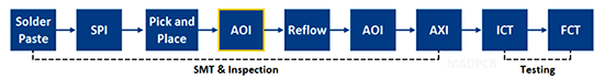
SMT, Inspection and PCBA Testing Process
The printed circuit board (PCB) assembly process typically consists of two parts: SMT &Inspection, and PCBA Testing.
spi aoi axi ict
Solder Paste Inspection -SPI
Solder Paste Inspection (SPI) is mainly done to check the solder paste deposits on the bare PCB board. The solder paste printing process is one of the most important parts of surface mount assembly process. The earlier one defect is identified, the less it will cost to correct -a useful rule to consider is that one fault identified after reflow cost, 10 times the amount to rework than that identified before reflow; a fault identified after test will cost one further 10 times more to rework.
For ensuring the desired amount of solder paste has been deposited without defects and that the process is repeatable, it is important to have a thorough and reliable inspection method –solder paste inspection (SPI), which is recommended to fully inspect every printed circuit board (PCB) before starting the component pick-and-place process. Solder paste inspection has the ability to not only check for solder paste area coverage and shorts, but also can accurately measure the shape and volume of the solder paste deposits.
With the SPI technology, SMT manufacturers can easily monitor the solder paste printing quality, reduce solder paste printing error, and ensure the component placement quality. It’s said that 80% PCB assembly defects are caused by improper solder paste printing. The aim of performing SPI process is to prevent from such defects. The CCD cameras in SPI system are used to take photos of the printed solder paste, which can be used to measure the alignment and volume of the solder paste applied. If found solder paste printing defects, SMT manufacturer can take the printed boards out from the SMT production line, and remove the deposited solder paste, then re-print the solder paste till ensure the deposit is ok to the quality norm. In SPI process, the engineer can find setup problem, and correct the solder paste printing setup.
The SPI process helps manufacturing defect-free PCB assemblies, and save significant SMT cost in high-volume assembly projects. In addition to this, it also contributes to reduce the lead time of your PCBA project, especially in volume production. For an error-free solder paste printing, it is therefore, recommended to implement SPI process.
Automated Optical Inspection -AOI
AOI, is the abbreviation of Automated Optical Inspection, an automated visual inspection system, which uses a camera to take high definition (HD) photos of the PCB board with solder paste printed but before reflow soldering, then use its computer vision to perform 100% inspection of the components and provides two types of data. One is attributes of part missing, misplacing, and wrong orientation. The other is variable to positional information, regarding the measured position of the part relative to its expected X/Y and the placement.
Before AOI technology applied, SMT manufacturers conduct this inspection with naked eye manual visual inspection, in which using a magnifying glass or microscope and a visual inspection by the operator to determine if the assembled PCB is unqualified, and to determine when correction operations are required. With the development of AOI technology, visual inspection with naked eye has become less and less feasible.
AOI bases on the optical principle, comprehensive use of photo acquisition, software analysis and other technologies, the SMT assembly manufacturing of defects encountered in the detection and image processing, is a relatively advanced method to confirm the manufacturing defects. SMT lines usually conduct AOI before and after reflow soldering, where the cost of correcting defects is the lowest and the efficiency is the highest.
- Pre-reflow AOI: If component faults found before the boards go to the reflow oven, the manual inspectors will review each fault and fix the component problems. Boards with placement defects will be repaired by the operators, then are reinserted into rail before pre-reflow AOI. Any new faults caused by the operator are found by the pre-reflow AOI system, the boards are returned one more time for repair. The cycle continues until each PCB board passes optical inspection.
- Post-Reflow AOI: Although we conduct SPI and pre-reflow AOI before reflow soldering, there is still in risk of some other assembly defects that the reflow may introduce. When boards go outside of at reflow oven, a post-reflow AOI can inspect all fault types, solder-related and component-level, at the end of the SMT production line. At this point, all boards can be manually fixed and some coarse level, time-delayed information can be feedbacked to the in-process side. Finding the last faults at the end of the SMT process will be time- and cost-saving for manufacturers because the PCB assembly defects at last will be at very low quantities after SPI and pre-reflow AOI processes.
“80% PCB assembly defects are caused by improper solder paste printing.” So, the defects detection before reflow oven is very important. Most post-reflow defects are already on the board before they go into the oven, all the oven does is to expose these defects. Not all SMT lines need combination of pre-reflow AOI and post-reflow AOI. If only use one AOI, where to put it? It is decided by the largest problem or top 3 problems in the whole assembly process. Besides, post-reflow AOI will find all defects at the end of the line. If find all defects at the end, it will cost much more for the manufacturer.
Automated X-ray Inspection -AXI
AXI works very well in electronics manufacturing for printed circuit boards where joints are visible. However, many PCBs today are using technologies such as BGA, BGA integrated circuits (ICs) and chip scale packages (CSPs) where the solder connections are not visible by visual inspection, like naked eye and AOI. This has arisen a result of the need for greater numbers of interconnections to integrated circuit packages and as a general result of increasing complexity. In these and many other instances, it is necessary to carry out checks using X-ray technology.
Automated X-Ray Inspection (AXI) is very similar to AOI, however instead of processing optical images, it uses computer vision with X-Ray images. This allows for the test to validate all solder connections on the board after assembly, including solder joints that are hidden underneath a component. This is useful for validating that ball grid array (BGA) components have been correctly assembled.
Flying Probe and In-Circuit Testing -ICT
Both flying probe and in-circuit test (ICT) use the same methodology for testing a DUT. These test methods use test probes to measure the resistance, capacitance, and other basic qualities between test points on the DUT. Both the flying probe and ICT tests are typically performed without having to apply power to the DUT.
Ideally, a test point is available on each net of the DUT, which will then enable this type of test to fully validate that no shorts or opens are on the DUT and that the components have all been placed in the correct locations.
A flying probe tester uses robotic test probes to quickly iterate through each test point and take measurements between it and every test point, this process can take up to 30 seconds. No custom fixtures are needed to use a flying probe tester, which makes it a great way to perform some electrical testing on low-volume PCB assembly runs of circuit boards.
In high-volume PCB assembly, when larger volumes are being produced, an in-circuit tester (ICT) is typically used. This type of system uses a bed-of-nails, containing many different probes which contact every test point on the DUT. The bed-of-nails fixture that is used in an ICT system has to be custom designed for each DUT, and this added cost and development time make them common for only mass-produced PCBAs. These fixtures perform the same tests that a flying probe system performs but in a short time.
Comparison of the Major Detection Capabilities of AOI, X-Ray and ICT
| Defect Type | AOI | X-Ray | ICT |
| Soldering Defects | |||
| Open Circuits | Y | Y | Y |
| Soldering Openings | Y | Y | Y |
| Solder Shorts | Y | Y | Y |
| Insufficient Solder | Y (not heel of joint) | Y | N |
| Solder Void | N | Y | N |
| Excess Solder | Y | Y | N |
| Solder Quality | N | Y | N |
| Component Defects | |||
| Lifted Lead | Y | Y | Y |
| Missing Component | Y | Y | Y |
| Misaligned or Misplaced Component | Y | Y | Y |
| Incorrect Component Value | N | N | Y |
| Faulty Component | N | N | Y |
| BGA and CSP Defects | |||
| BGA Shorts | N | Y | Y |
| BGA Open Circuit Connections | N | Y | Y |