Table of Contents
Through Hole ‧ Axial & Radial
Capacitor (Non-Polarized)
Description: Capacitor store and discharge electricity. They consist of two metal plates, or conducting surfaces, separately by an insulating material called a dielectric. After a sufficient buildup in one plate, the charge is felt in the opposite plate. There are four basic types of non-polarized capacitors:
- Ceramic disc-radial
- Dipped mica-radial
- Mylar-radial, usually round or oval bodles
- Glass-packed, axial, easy to mistake or diode or resistor
Class Letter: C (non-polarized)
Prefix: None
Value Code: Measured in microfarads (μF), nanofarads (nF) or picfarads (pF). The value is printed on the capacitor body using some form or abbreviation. Also specified is the operating voltage for the capacitor. These two values determine the physical size of the component.
Tolerance: Printed as percentage (example +/-5%) or as letter scheme.
Orientation: None
Capacitor (Polarized)
Description: Polarized capacitors function in the same way as non-polarized capacitors.
Class Letter: C
Other: C
Value Code: Measured in microfarads (μF), nanofarads (nF), or picofarads (pF). The value is printed on the capacitor body using some from of abbreviation. Also specified is the operating voltage for the capacitor. These two values determine the physical size of the component.
Tolerance: Printed as percentage (example: +/-5%) or as letter scheme.
Orientation: By polarity. A Square Land on PCB may mark where the positive lead (anode) is to be inserted.
Polarity: Polarized capacitors can be both axial or radial and will have one lead marked as positive (+). This positive lead can be marked or formed in several ways.
Symbols:
- Plus (+): marks positive lead
- Dot (·): marks positive lead
- Band: marks positive lead
- Line: the line can have pluses (+) leading to the positive leg or minuses (-) leading to the negative leg.
- Arrows: arrows down the side lead to the negative end.
Colors:
- Silver Square: marks positive lead
- Colored End: marks positive lead
- Shapes and Forms:
- Ridge or Bevel: marks positive lead
- Groove: marks positive lead
- Bubble: marks positive lead (if both ends have a bubble, the larger one is positive.)
- Larger Lead: the PCB holes are sized to match the larger lead.
Variable Capacitor
Another type of polarized capacitor is the aluminum electrolytic capacitor. These capacitors have a larger capacitance per unit volume than other types, marking them valuable irrelatively high-current and low-frequency electrical circuits -such as power supply filters. The dielectric is a thin layer of aluminum oxide.
Description: These capacitors can change capacitance by turning a screw that causes the plates to move closer or further apart. The closer the plates, the higher the capacitance.
Class Letter: C
Other: C VAR, C ADJ
Prefix: None
Value Code: Measured as a range, such as 27-200μF.
Tolerance: None
Orientation: Non-symmetrical lead pattern allows it to be installed only one way.
Polarity: None
Crystal Oscillator
Description: Crystal Oscillators usually have metal bodies and produce a consistent electrical pulse. They are typically used as clocks, controlling the timing of events in digital circuits.
Class Letter: L
Other: B
Prefix: None
Value Code: Measured in megahertz (MHz), or kilohertz (KHz)
Tolerance: None
Orientation: Angled corner or dot
Polarity: None
Diode
Description: Diodes are semiconductors that only allow current to flow in to flow in one direction -like a one-way street. They can convert alternating current to direct current. A Zener diode acts as a voltage limiter for DC voltages. A diode’s part number is usually specified by the prefix 1N, followed by two- to four- digit numbers. Examples include 1N53, 1N751 and 1N4148.
Class Letter: D or CR
Other: Y
Prefix: 1N
Value Code: None
Orientation: By polarity
Polarity: Polarity is usually indicated by colored ring or up to three rings near the negative (cathode) end of axial diodes. An arrow may also point to the negative end. The PCB is marked with a stripe, line, or arrow symbol showing where the cathode end of the diode should be placed. A Square Land may also mark where the cathode end is inserted.
Light-Emitting Diode
Description: Also known as LEDs, these components emit light
Class Letter: DS
Other: E, LED, D, DIS, CR
Prefix: None
Value Code: None
Orientation: By Polarity
Polarity: LEDs are typically radial leaded, and polarity is indicated by a short lead, a flat side to the component housing, or position of the cup and spoon. The cathode is usually identified by the shorter lead, or by a flat side (if any) to the LED housing. The cup inside the lens is sometimes associated with the cathode lead, and the spoon with the anode, but this may vary with some manufacturers.
Square Land: The PCB may also be marked with a square land showing where the cathode end is inserted and/or a silkscreened outline of the component body with a flat edge to indicate polarity.
Filter
Description: Filters are used to pass one frequency or frequency band while blocking others. They are often used to filter electrical noise in a circuit.
Class Letter: FL
Other: L
Prefix: None
Value Code: None
Tolerance: None
Orientation: The installation of filters is usually by lead configurations. The pattern of holes or lands on the PCB means there is only one way to insert the filter.
Polarity: None
Fuse /Circuit Breaker
Description: Fuses consist of a wire with low melting point metal. When current passing through the wire exceeds a prescribed level, the wire melts and opens the circuit, protecting equipment from damage. A circuit breaker is a device that when exposed to excess current will “trip” or become electrically open and can be reset.
Class Letter: F
Prefix: None
Value Code: Measured in amps
Tolerance: None
Orientation: None
Polarity: None
Class Letter: CB
Inductor / Coil
Description: Inductors consist of a coil of wire that creates a magnetic field when current flows through the coil. Transformers, Coils and Toroids are related to inductors (see Transformers). The toroid choke consists of a coild wound on a toroid, or doughnut of magnetic metal. The metal core increases the inductance of the coil.
Class Letter: L
Prefix: None
Value Code: Measured in microhenry (μH) or millihenry (mH). The value is either printed on the inductor body or calculated by decoding 4 of 5 colored bands on the inductor body into numbers.
Tolerance: Printed as last of five-band color band system.
Orientation: None
Transformer
Description: Transformers are related to inductors. Transformers basically consist of primary and secondary colis wound on a common core of ferromagnetic material. When alternating current flows through the primary coil, the resulting magnetic field induces an alternating voltage across the secondary coil. The induced voltage can cause current to flow in an external circuit.
Class Letter: L
Prefix: None
Value Code: Measured in microhenry (μH) or millihenry (mH). The value is printed on the body.
Orientation: Many transformers have non-symmetrical leads which only allow it to be installed one way.
Resistor
Description: Resistors limit the flow of electrical current in a circuit. This is like a highway narrowing from six lanes to a two-lane road. Fixed resistors are usually made of metal film. The bigger the metal film resistor, the greater its wattage rating (wattage is a measure of electrical power). Resistors can also be made of hot molded carbon.
Class Letter: R
Prefix: RC=Color Coded, RN=Metal Film, RCL=Wire Wound
Value Code: Measured in ohms. The value is either printed on the resistor body or is calculated by decoding 3 to 5 colored bands on the resistor body into numbers.
Tolerance: Printed on body or as part of color band system.
Orientation: None
Polarity: None
Variable Resistor
Description: Also called a potentiometer, trimpot or trimmer, a variable resistor is a resistor whose value can be changed by tuning a shaft, screw or sliding a contact.
Class Letter: R
Other: YR, VAR, VRN, ADJ
Prefix: None
Value Code: Measured in a range in ohms. Maximum value is usually molded into component body. Example: 20MΩ.
Tolerance: None
Orientation: Non-symmetrical lead pattern only allowed it to be installed one way. Pin one is usually identified. A square land may also mark where pin one is inserted.
Polarity: None
Voltage Regulator
Description: Voltage regulators keep output voltage constant during variations of the output load or the input voltage. The package configuration often looks like a TO-220.
Class Letter: YR
Other: U
Prefix: None
Value Code: None
Tolerance: None
Orientation: Angle on the body or indented dot.
Polarity: None
Transistor
Description: Transistors are semiconductors that can amplify, oscillate and provide switching action on electrical signals. Like diodes, transistors do no utilize units of measurement. Instead, their component type is usually specified by the prefix 2N or 3N, followed by two- to four-digit numbers. Examples include 2N50, 2N701 and 2N2222A.
Class Letter: Q
Other: Y or U
Prefix: 2N
Orientation: Indicated by one of several methods:
- Pin Numbers or pin names which match to the PCB silkscreen.
- Tab on the transistor “can”. When looking down on the component from the top, pin one is either to the right of, or directly underneath the tab. The pins count counterclockwise from pin one.
- Matching component shape with PCB silkscreen outline. Outline on PCB includes the tab -align the tab. Outline on PCB includes the flat side of the transistor -align the flat side. Pattern of through holes on PCB means there is only one way to insert the transistor.
Switch / Relay
Description: Switches open and close a circuit.
Class Letter: S
Other: SW
Prefix: None
Value Code: May have value rating for maximum current in amps. Example: 10A. May also have mechanical information such as DPDT (Double Pole Double Throw) printed on it.
Tolerance: None
Orientation: Dot or notch
Polarity: None
Description: Relays are switches that open and close when actuated by an applied signal.
Class Letter: K
Through Hole ‧ Hardware
Connector
Description: Connectors are placed on a PCB so that wires, cables and other outside connections can be made to the PCB. They usually have a housing around their pins.
Class Letter: P for MALE PLUG connector, or J for FEMALE JACK / RECEPTACLE connector.
Other: None
Header
Description: Headers, like connectors are placed on a PCB so that outside connections can be made. Headers usually do not have a housing around their pins.
Class Letter: J or P
Orientation: Usually none. Often has alignment or locking tabs for the connector which mates with it. Correct orientation of this tab is important.
Polarity: None
Jumper
Description: Also called jumper configuration, jumper wire or head pin configuration. Jumpers connect two pins on the assembly together, providing an electrical path between those points. Jumpers are sometimes used to solve circuitry errors in the PCB itself. Other times they are used to provide a way to change the assembly’s configuration for different applications.
Class Letter: W, or E for insulated piece of conductor (wire); or P, for a plug.
Other: JP
Prefix: None
Value Code: None
Tolerance: None
Orientation: Jumper goes into header socket
Polarity: None
Socket
Description: Sockets are soldered onto circuit boards so that an IC can be plugged into the socket and not soldered directly to the board. This makes removing or upgrading the part much easier. Sockets are sometimes used for components that cannot be soldered in place because of heat sensitivity.
Class Letter: X, XAR, XU, XQ, etc.
Other: TS, S
Prefix: None
Value Code: None
Tolerance: None
Orientation: Sockets usually have a dot or a notch to indicate orientation to the PCB. Once installed, a socket may cover the PCB orientation mark, so it’s important to place the socket correctly.
Through Hole ‧ IC’s
SIP
Description: SIP stands for Single-In—line-Package. SIPs are often resistor networks (or packs) diode arrays, power converters and power regulators. PSIP stands for a Plastic SIP.
Class Letter: R for resistor networks, D or CR for diode array, etc.
Other: PR, RN
Prefix: None
Value Code: SIP packages sometimes include banks of passive components. Those values may be marked on the component package. For example, eight 2K resistors would have the value: “8x2K”.
Tolerance: None
Orientation: Determined by the location of lead one. A SIP IC’s leads are numbered to ensure proper placement of the component on the circuit board or into a PCB-mounted socket. The orientation marking on most SIPs is usually right over lead one. The remaining leads are counted from lead one.
Lead One Markings: The most common markings for orientation on SIPs are numbers, a stripe or a dot.
DIP
Description: DIP standards for Dual-In—line-Package. DIPs are usually made of plastic (called PDIPs) or ceramic (called CERDIPs). They may include hundreds, or thousands of various components. Also includes Shrink DIPs (SDIPs).
Class Letter: U
Other: IC or AR, C, Q, R, etc.
Prefix: None
Value Code: DIP packages sometimes include banks of passive components. Those values may be marked on the component package. For example, eight 2K resistors would have the value: “8x2K”.
Lead Pitch: 100mils DIPs and 70mils SDIPs.
Orientation: Determined by the location of lead one. A DIP IC’s leads are numbered to ensure proper placement of the component on the circuit board or into a PCB-mounted socket. The orientation marking on most DIPs is usually either right over lead one or one the ends at which lead one is found. The remaining leads are counted counterclockwise from lead one.
Lead One Markings: The most common markings for orientation on ICs are:
- Notch
- Numbers
- Stripe
- Dimple
- Wedge
Square Land: The square land is used to show the location of lead one on the PCB. Aligning lead one of the IC with the square land on the board ensures proper installation of the component.
IC Can
Description: IC Cans are often transistors or voltage regulators.
Class Letter: U general IC, Q for transistor, AR amplifier, etc.
Other: IC
Prefix: None
Value Code: None
Tolerance: None
Orientation: Determined by the location of lead one. An IC Can’s leads are numbered to ensure proper placement of the component on the circuit board or into a PCB mounted socket. The orientation marking on most IC Cans is usually a tab in the rim of the can over the highest numbered pin, or between pin one and the highest pin. The pins are counted counterclockwise starting from the right of the tab when looking down on the top of the can.
PGA
Description: PGA standards for Pin Grid Array. PGAs have several rows of leads or pins extending from the bottom of the IC. The rows make up a grid of connection points. PGAs come in plastic packages (PPGA) and ceramic packages (CPGA).
Class Letter: U
Other: IC or AR, C, Q, R, etc.
Prefix: None
Value Code: None
Tolerance: None
Orientation: Usually determined by the location of a notch in the package right over pin one. A corresponding mark on the PCB or socket provides proper alignment. Sometimes also by a missing pin on the component, or a missing hole on the board.
Square Land: A square bae to one lead among the leads in a PGA is also used to show orientation. Aligning that lead with a matching square land on the board ensures proper installation of the component.
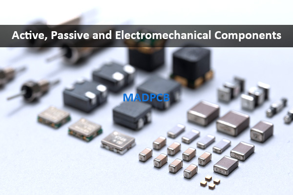
Surface Mount ‧ CHIPS, MELFs & SOTs
Chip Component
Description: Chip components are usually ceramic-bodles packages with metal connections called terminations at either end. The most common types of chip components are ceramic resistors and capacitors. Five-sided chip components have a solderable surface on three sides of its terminal contact.
Class Letter: R
Value: Measured in ohm (Ω)
Orientation: None
Polarity: None
Chip Resistors
Class Letter: C
Value: Measured in microfarads (μF) or picofarads (pF).
Orientation: None
Polarity: None (Note: See Tantalum Capacitors)
Chip Components / Resistor
Sometimes the number value (Ohms) may be printed on the chip resistor body. More frequently, this value is printed on the label of the reel in which the chips are packaged. This is because the component itself is too small or will not allow for printing on the resistive element.
The code is a three- or four-digit number. With three-digit codes, the first two numbers are value numbers, and the third is the multipliers. For example, 102, where 1 and 0 are attached to 2 zeros to equal 1000 ohms.
With four-digit codes, the first three numbers are the value numbers, and the fourth number is the multiplier. For example: 1501, where 1, 5, and 0 are attached to 1 zero to equal 1500 Ohms.
For either code, a “0” (zero), in the multiplier position means don’t add any zeros. Example: 150, where 1 and 5 are attached to no zeros to equal 15 Ohms.
A letter R in either code means to place a decimal point at this spot. Example: 49R9 = 49.9Ohms.
| Tolerance Letter Codes | |
| B=+/-.1% | For some manufacturers, chip resistors with 3-digit codes are assumed to be 5% tolerance, and 4-digit chips are assumed to be 1%.
Tolerance can be decoded from this chart when letter codes are used. |
| C=+/-.25% | |
| D=+/-.5% | |
| F=+/-1% | |
| G=+/-2% | |
| J=+/-5% | |
| K=+/-10% | |
| M=+/-20% | |
| Z=+80%/-20% | |
Chip Components / Capacitor
Reading Chip Capacitor Value Codes
Depending on the size of the chip capacitor, the value code may be printed on the body of the component, or on the label of the reel in which they’re packaged. The code for a chip capacitor is a three-digit number expressing a value, usually in picofarads (pF).
As with chip resistor three-digit codes, the first two numbers are value numbers, and the third is the multiplier. Example: 221, where 2 and 2 are attached to 1 zero to equal 220 pF.
A “O” (zero) in the multiplier position for capacitors means no zeros are added to the value. A letter R is a decimal point holder. Tolerance comes in many varieties and may be shown with letter codes using the key chart at the bottom of the previous page.
Chip Component /Size Codes
A chip’s size, in inches or millimeters, is described by a 4-digit code. The first 2 digits are the length. The second 2 digits are the width.
| Size Codes (Inches) | Size Codes (metric) | ||
| 0402 | .04’’ x .02’’ | 1005 | 1.0 x 0.5mm |
| 0603 | .06’’ x .03’’ | 1508 | 1.5 x 0.8mm |
| 0805 | .08’’ x .05’’ | 2012 | 2.0 x 1.2mm |
| 1005 | .10’’ x .05’’ | 2512 | 2.5 x 1.2mm |
| 1206 | .12’’ x .06’’ | 3225 | 3.2 x 2.5mm |
| 1210 | .12’’ x .10’’ | 4532 | 4.5 x 3.2mm |
| 1812 | .18’’ x .12’’ | 5664 | 5.6 x 6.4mm |
| 2225 | .22’’ x .25’’ | – | – |
Tantalum Capacitor
Description: Molded Tantalum Capacitors are polarized chip capacitors with inward formed L-leads. These leads almost touch the body of the component. Inside are metal plates which store and discharge electricity.
Class Letter: C
Prefix: None
Value Range: 0.001μF to 1000pF, 4 to 100V DC
Tolerance: None
Orientation: By polarity
Polarity: Line, + or A on anode end. Beveled top on anode end.
Size Code: A tantalum capacitor’s size is described by one of four letters: A, B, C, or D. These four size codes stand for metric footprint of length and width.
| Tantalum Capacitor
Size Codes |
| A = 3.2 x 1.6mm
B = 3.5 x 2.8mm C = 6.0 x 3.2mm D = 7.3 x 4.3mm |
MELF
Description: Metal Electrode Face (MELF) leadless components have metallized terminals at both of a cylindrical body. Typical MELF components include diodes, resistors, capacitors and inductors. Polarity, value coding and CRDs are the same for these components as for their smallest of the MELFs are called “mini-MELFs” and “micro-MELFs”.
Class Letter: Depends on component type
Prefix: None
Value Code: Resistors have 4 or 5 bands which convey their value.
Tolerance: Resistors have a tolerance band.
Orientation: By polarity
Polarity: MELF diodes have a band at the cathode end.
Sizes: MELF resistors are designed to fit same footprints as chip resistors, such as the 0805 (.08’’ x .05’’) and the 1206 (.12’’ x .06’’).
SOT / SOD
Description: Small Outline Transistor (SOTs) and Small Outline Diodes (SODs) are rectangular transistor or diode packages with three or more gull wing leads. The most popular size is the SOT23. Other package sizes include the SOT89, SOT143 and SOT223. SOTs have 3 or 4 gull wings on two sides of their package.
Class Letter: Q for transistor packages; D or CR for diode packages.
Prefix: None
Tolerance: None
Orientation: Determined by lead pattern, or number one lead.
Polarity: None
DPAK
Description: DPAKs are Diode Packages, which accommodate higher powered groups of transistor and diodes. D2PAKs are the largest surface mount transistor made and include a heat sink mounting pad. DPAKs have a termination on one side of the package, and 2 or 3 gull wings on the opposite side.
Class Letter: Q for transistor packages; D or CR for diode packages.
Prefix: None
Tolerance: Determined by package size.
Orientation: Determined by lead pattern.
Polarity: None
Sizes: SOTs and DPAKs are designed to fit the same footprint as their through hole cousins. For instance, a D2PAK is designed to fit the TO220 through hole transistor.
Surface Mount ‧ Dual Inline SOICs
SOIC / SOP
Description: SOIC stands for Small Outline Integrated Circuit, and SOP stands for Small Outline Package. These two abbreviations are used Interchangeably. The SOIC (SOP) family is made up of variety of Dual In-Line (leaded on 2 sides) rectangular body sizes several lead pitches and lead styles. The SOIC started out in the English system (mil), but as the family grew and the pitches decreased from 50mil, the new packages were standardized in the metric (mm) system. The number of leads on each package can change and the maximum is determined by the body length and the lead pitch. The actual individual SOIC package is referred to by its abbreviation which rarely includes an “IC” at the end. This makes for some confusion as the same package may be called by more than one name by different companies. For instance, a SOIC and a SOLIC are both names for the same IC – a Small Outline Large IC.
# of Pins: 5-96
Body Width: Various
Lead Type: Gull Wing, J-lead, flat and L-lead
Lead Pitch: From 1.27mm (50mils) to 0.4mm
Class Letter: U
Other: IC or AR, C, Q, R, etc.
Value: None
Orientation: Indicated by a dot or a beveled edge over the number one lead, or an end notch or stripe on the IC. Leads are counted counterclockwise from the number one lead. The PCB often has a square silkscreened at the pin one location.
SO
Description: SO stands for Small Outline. This is the original narrow body SOIC.
# of Pins: 4-16
Body Width: 49mil (1.25mm), 63mils (1.60mm), 154mils (3.90mm), 175mils (4.40mm)
Lead Type: Gull Wing
Lead Pitch: 50mil (1.27mm), 1.25mm, 0.95mm
Class Letter: U
Other: IC or AR, C, Q, R, etc.
Value: None
Orientation: Indicated by a dot or a beveled edge over the number one lead, or an end notch or stripe on the IC. Leads are counted counterclockwise from the number one lead. The PCB often has a square silkscreened at the pin one location.
Polarity: None
SOM
Description: SOM stands for Small Outline Medium (body width). Commonly used for resistor networks.
# of Pins: 8-16
Body Width: 220mils (5.60mm)
Lead Type: Gull Wing
Lead Pitch: 50mil (1.27mm)
Class Letter: U
Other: IC or AR, C, Q, R, etc.
Value: None
Orientation: Indicated by a dot or a beveled edge over the number one lead, or an end notch or stripe on the IC leads are counted counterclockwise from the number one lead. The PCB often has a square silkscreened at the pin one location.
Polarity: None
SOL / SOW
Description: SOL stands for Small Outline Large, and SOW stands for Small Outline Wide. These two abbreviations are used interchangeably.
# of Pins: 14-70
Body Width: 209mils (5.30mm), 295mils (7.50mm), 300mils (7.62mm), 330mils (8.40mm), 350mils (8.90mm), 390mils (9.90mm), 440mils (11.20mm), 500mils (12.70mm), 525mils (13.30mm)
Lead Type: Gull Wing
Lead Pitch: 50mil (1.27mm), 1.00mm, 0.80mm
Class Letter: U
Other: IC or AR, C, Q, R, etc.
Value: None
Orientation: Indicated by a dot or a beveled edge over the number one lead, or an end notch or stripe on the IC. Leads are counted counterclockwise from the number one lead. The PCB often has a square silkscreened at the pin one location.
Polarity: None
SOJ / SOL-J
Description: SOJ stands for Small Outline J-lead and SOL-J stands for Small Outline Large- J-lead. These two abbreviations are used interchangeably.
# of Pins: 24-70
Body Width: 300mils (7.62mm), 350mils (8.90mm), 400mils (10.16mm), 500mils (12.70mm), 630mils (16.00mm)
Lead Type: J-lead
Lead Pitch: 50mil (1.27mm), 1.00mm, 0.80mm
Class Letter: U
Other: IC or AR, C, Q, R, etc.
Value: None
Orientation: Indicated by a dot or a beveled edge over the number one lead, or an end notch or stripe on the IC. Leads are counted counterclockwise from the number one lead. The PCB often has a square silkscreened the pin one location.
Polarity: None
SSOP / VSOP / TSSOP
Description: SSOP -which stands for Shrink Small Outline Package -and VSOP -which stands for Very Small Outline Package -are used interchangeably. These are higher density (pitch) gull wing leads. TSSOP stands for Thin Shrink Small Outline where the package profiles are only allowed to have a total height of 1.00mm.
# of Pins: 8-68
Body Width: 154mils (3.90mm), 4.40mm, 209mils (5.30mm), 6.10mm, 8.00mm.
Lead Type: Gull Wing
Lead Pitch: 0.65mm, 0.50mm, 0.40mm
Class Letter: U
Other: IC or AR, C, Q, R, etc.
Value: None
Orientation: Indicated by a dot or a beveled edge over the number one lead, or an end notch or stripe on the IC. Leads are counted counterclockwise from the number one lead. The PCB often has square silkscreened at the pin one location.
Polarity: None
QSOP
Description: QSOP stands for Quarter Small Outline Package. This is the same as the SO except it only has 25mil pitches instead of 50. These are higher density (pitch) gull wing leads.
# of Pins: 14-64
Body Width: 154mils (3.90mm), 300mils (7.62mm)
Lead Type: Gull Wing
Lead Pitch: 25mils (0.65mm)
Class Letter: U
Other: IC or AR, C, Q, R, etc.
Value: None
Orientation: Indicated by a dot or a beveled edge over the number one lead, or an end notch or stripe on the IC. Leads are counted counterclockwise from the number one lead. The PCB often has a square silkscreened at the pin one location.
Polarity: None
TSOP
Description: TSOP stands for Thin Small Outline Package. They come in two types. The Type I package has leads on the short sides of the rectangular component. Type II has leads on the long sides, just like all other SO packages. TSOPs are typically used for memory applications, such as DRAM and Flash memory. These thin profile packages are only allowed to have a total height of 1.00mm.
# of Pins: Type I: 24-56, Type II: 20-100
Body Width: Type I: 6.00mm, 8.00mm, 10.00mm, 12.00mm, 14.00mm; Type II: 300mil (7.62mm), 400mil (10.16mm), 500mil (12.70mm), 630mil (16.00mm).
Lead Type: Gull Wing
Lead Pitch: Type I: 0.50mm and 0.56mm; Type II: 1.27mm, 0.80mm, 0.65mm, 0.50mm, 0.40mm
Class Letter: U
Other: IC or AR, C, Q, R, etc.
Value: None
Orientation: Indicated by a dot or a beveled edge over the number one lead, or an end notch or stripe on the IC. Leads are counted counterclockwise from the number one lead. The PCB often has a square silkscreened at the pin one location.
Polarity: None
Flat Lead Small Outline and Quad Package
Description: Flat lead package have leads that extend from the bottom plane of the component -normally from two sides -so they are most often Small Outline (SO). There are times when a Flat lead may have four sides (QUAD).
# of Pins: 4-28
Body Width: Various sizes, but the most popular are 209mils (5.30mm) or the 300mils (7.62mm) SO.
Lead Type: Flat
Lead Pitch: 50mil (1.27mm)
Class Letter: U
Other: IC or AR, C, Q, R, etc.
Value: None
Orientation: Indicated by a dot or a beveled edge over the number one lead, or an end notch or stripe on the IC. Leads are counted counterclockwise from the number one lead. The PCB often has a square silkscreened at the pin one location.
Surface Mount ‧ Peripheral Loaded Quads
PLCC
Description: PLCC stands for Plastic Leaded Chip Carrier, which is a peripheral leaded QUAD family with J-bend type leads. The family has both square and rectangular configurations. PLCCs can either be put into sockets or soldered directly on to circuit boards. The ceramic version of this IC package is called a CLCC (Ceramic Leaded Chip Carrier). This family is sometimes confused with LCCC (Leadless Ceramic Chip Carrier) which is a leadless component.
Lead Type: J-lead
# of Pins: Square: 20-100; Rectangular: 18-32
Body Width: Square: .390’’, .490’’, .690’’, .990’’, 1.190’’ & 1.300’’; Rectangular: .322’’ x .462’’, .328’’ x .528’’, .390’’ x .590’’ & .490’’ x .590’’.
Lead Pitch: 50mil (1.27mm)
Class Letter: U
Other: IC or AR, C, Q, R, etc.
Value: None
Orientation: Indicated by a dot or a beveled edge over the number one lead, or an end notch or stripe on the IC. Leads are counted counterclockwise from the number one lead. The PCB often has a square silkscreened at the pin one location.
QFP / MQFP / FQFP / CQFP
Description: QFP stands for Quad Flat Pack, MQFP stands for Metric Quad Flat Pack, and FQFP stands for Fine Pitch Quad Flat Pack. This family was developed during the time that surface mount packages were evolving from English to Metric dimensioning. These are peripheral leaded QUAD (4-sides) packages with gull wing lead types that are metric pitches. The family has both square and rectangular configurations. QFPs have higher lead counts than PLCCs and have finer pitches from a high of 1.00mm to a low of 0.40mm. MQFPs have pitches of 0.50mm and 0.40mm. A ceramic body, internal multilayer version of the QFP is called a CQFP.
# of Pins: Square: 36-376; Rectangular: 64-128.
Body Width: Square: 10, 12, 14, 20, 28, 32, 36 0.40mm; Rectangular: 20 x 14mm
Lead Type: Gull Wing
Lead Pitch: 1.00mm, 0.80mm, 0.65mm, 0.50mm and 0.40mm
Class Letter: U
Other: IC or AR, C, Q, R, etc.
Value: None
Orientation: Indicated by a dot or a beveled edge over the number one lead, or an end notch or stripe on the IC. Leads are counted counterclockwise from the number one lead. The PCB often has a square silkscreened at the pin one location.
LQFP / TQFP
Description: LQFP stands for Low Profile (1.2mm maximum) Quad Flat Pack and TQFP stands for Thin Profile (1.00mm maximum) Quad Flat Pack. This family was developed during the time that surface mount packages were evolving from English to Metric dimensioning. These are peripheral leaded QUAD (4-sided) packages with gull wing lead types that are all metric pitches. The family has both square and rectangular configurations. The LQFP and TQFP share the same body sizes, pitches, and lead counts with the exception that the 28 x 28mm bodles are only made using the LQFP body thickness.
# of Pins: Square: 20-256; Rectangular: 64-128
Body Width: Square: 4, 5, 7, 10, 12, 14, 20, 24 & 28mm; Rectangular: 20 x 14mm
Lead Type: Gull Wing
Lead Pitch: 1.00mm, 0.80mm, 0.65mm, 0.50mm and 0.40mm
Class Letter: U
Other: IC or AR, C, Q, R, etc.
Value: None
Orientation: Indicated by a dot or a beveled edge over the number one lead, or an end notch or stripe on the IC. Leads are counted counterclockwise from the number one lead. The PCB often has a square silkscreened at the pin one location.
Polarity: None
FQFP / BQFP
Description: PQFP stands for Plastic Quad Flat Pack. The PQFP was the first QFP published by JEDEC as a package outline standard, and was a fine pitch gull wing version of a PLCC. The bumpers on the end of the package were there to add mechanical protection for the fine pitch gull wings during handling and assembly. Sometimes these packages were called BQFP which would have been Bumpered Quad Flat Pack. PQFPs are built with true inch measurements of their lead pitch. The 25mil lead pitch version when converted to metric is .635, which is not a hard metric pitch and is not used in the industry. PQFPs are all square-bodles packages.
# of Pins: 44-132
Body Width: Square: .390’’, .490’’, .690’’ & .1.190’’
Lead Type: Gull Wing
Lead Pitch: 25mm
Class Letter: U
Other: IC or AR, C, Q, R, etc.
Value: None
Orientation: Indicated by a dot or a beveled edge over the number one lead, or an end notch or stripe on the IC. Leads are counted counterclockwise from the number one lead. The PCB often has square silkscreened at the pin one location.
Polarity: None
LCC/LCCC
Description: LCC stands for Leadless Chip Carrier which is a peripheral leadless Dual and Quad family with bottom terminal pads and edge castellations. The family has both square and rectangular configurations. LCCs can either be put into sockets or soldered directly on to circuit bonds. They are most commonly used in aerospace, flight, military and other high reliability applications. The ceramic version of this IC package is called a LCCC (Leadless Ceramic Chip Carrier).
# of Pins: Square: 16-304; Rectangular: 4-32
Body Width: Square: .300’’, .350’’, .400’’, .450’’, .560’’, .650’’, .750’’, .950’’, 1.150’’, 1.350’’, 1.650’’ & 2.050’’; Rectangular: .150’’ x .220’’, .170’’ x .245’’, .290’’ x .500’’, .290’’ x .425’’, .450’’ x 550’’, .350’’ x .550’’, .285’’ x .350’’, and .285’’ x .425’’.
Lead Type: Solderable bottom terminal pads and castellations
Lead Pitch: Square: 50mil (1.27mm), 40mil (1.02mm), 25mil (.635mm) and 20mil (.508mm); Rectangular: 50mil (1.27mm)
Class Letter: U
Other: IC or AR, C, Q, R, etc.
Value: None
Orientation: Terminals or castellations are counted counterclockwise from number one. The PCB often has a square silkscreened at the number one location.
QFN
Description: QFN stands for Dual Flat No-lead, which are peripheral leadless dual packages with bottom terminal pads and possible edge castellations. The family has both square and rectangular configurations. QFNs are intended to be soldered directly on to circuit boards. Reference marketing names include MLF and MLP.
# of Pins: Square: 2-18; Rectangular: 4-28
Body Width: Square: 1.50mm, 2.00mm, 3.00mm, 4.00mm & 5.00mm; Rectangular: Numerous sizes from as small as 1.50 x 1.00mm to as large as 10.00 x 10.00mm.
Lead Type: Solderable bottom terminal pads.
Lead Pitch: Square: 0.95mm, 0.80mm, 0.65mm, and 0.50mm
Class Letter: U
Other: IC or AR, C, Q, R, etc.
Value: None
Orientation: Indicated by a dot or a beveled edge over the number one lead, or an end notch or stripe on the IC. Leads are counted counterclockwise from the number one lead. The PCB often has a square silkscreened at the pin one location.
QFN
Description: QFN stands for Quad Flat No-leas which are peripheral single row leadless quad packages with bottom terminal pads and possible edge castellations. The family has both square and rectangular configurations. QFNs are intended to be soldered directly on to circuit boards. Reference marketing names include MLF and MLP.
# of Pins: Square: 4-108; Rectangular: 8-40
Body Width: Square: 2.00mm, 3.00mm, 3.50mm, 4.00mm, 5.00mm, 6.00mm, 7.00mm, 8.00mm, 9.00mm, 10.00mm, and 12.00mm; Rectangular: Numerous sizes from as small as 3.50 x 4.50mm to as large as 7.00 x 9.00mm.
Lead Type: Solderable bottom terminal pads
Lead Pitch: Square: 0.80mm, 0.65mm, 0.50mm and 0.40mm
Class Letter: U
Other: IC or AR, C, Q, R, etc.
Value: None
Orientation: Indicated by a dot or a beveled edge over the number one lead, or an end notch or stripe on the IC. Leads are counted counterclockwise from the number one lead. The PCB often has a square silkscreened at the pin one location.
QFN / Multiple Rows
Description: QFN stands for Quad Flat No-lead and sometimes has multiple rows, which are peripheral two or three row leadless quad packages with bottom terminal pads and the outer row having possible edge castellations. These packages were created to take advantage of the QFN technology, but the applications required larger pin counts therefore additional row where added. The family currently has square configurations. QFNs are intended to be soldered directly on to circuit boards. Reference marketing names include MLF and MLP.
# of Pins: 44-396
Body Width: Square: 5.00mm, 6.00mm, 7.00mm, 8.00mm, 9.00mm, 10.00mm, 11.00mm, 12.00mm, 13.00mm, 14.00mm, and 15.00mm.
Lead Type: Solderable bottom terminal pads
Lead Pitch: 0.65mm, 0.50mm, and 0.40mm
Class Letter: U
Other: IC or AR, C, Q, R, etc.
Value: None
Orientation: Indicated by a dot or a beveled edge over the number one pad, or an end notch or stripe on the IC. Terminal pads are counted counterclockwise from the number one lead. The PCB often has a square silkscreened at the lead one location.
Surface Mount ‧ Area Arrays
BGA/ CBGA / PBGA / CCGA / LGA
Description: BGA stands for Ball Grid Array, which is an array family with balls as the bottom terminations. When the BGA has a ceramic substrate, it is called Ceramic Ball Grid Array (CBGA). When the BGA has a tape or laminate substrate, it is called a Plastic Ball Grid Array (PBGA). When a Ceramic Grid Array has Columns rather than balls, it is called a Ceramic Column Grid Array (CCGA). When a BGA or CGA is sold without balls or columns attached, it is called a Land Grid Array (LGA). The families have both square and rectangular configurations. All BGAs, CGAs and LGAs can either be put into sockets or soldered directly to circuit boards.
# of Pins: Ball or Ball Land: Square: 9-2404; Rectangular: 119-744; Column or Column Land: Square: 225-2916; Rectangular: 300-1230.
Body Width: Ball or Ball Land: Square from 7.00mm to 50.00mm; Rectangular: from 10.00mm x 18.00mm to 25.00mm x 32.50mm; Column or Column Land: Square from 25.00mm to 45.00mm; Rectangular: from 25.00mm x 32.50mm to 32.50mm x 42.50mm.
Lead Type: Solderable ball or lands
Lead Pitch: 1.50mm, 1.27mm (50mil) and 1.00mm
Class Letter: U
Other: IC or AR, C, Q, R, etc.
Value: None
Orientation: Indicated by a dot or a beveled edge over the A1 lead, or an end notch or stripe on the IC. Leads are counted using a grid system, starting with the A1 lead. The PCB often has a square silkscreened at the A1 location.
PoP
Description: PoP stands for Package on Package. This packaging concept was developed to provide flexibility to meet the increasing challenges for size and cost reduction while increasing signal processing performance and memory capabilities. The PoP in it simplest form ahs a bottom package which is normally the logic package and the upper package contains the memory components. The bottom package is a FBGA with FBGA lands on the top side lands. The PoP maybe shipped completed with the two packages assembled or shipped separately on to circuit boards.
# of Pins: Bottom Ball or Ball Land (bottom package) from 304-841; Top Ball Land (Bottom Package) and Ball Top Package: from 96-126.
Body Width: 10.00mm, 11.00mm, 12.00mm, 13.00mm, 14.00mm, and 15.00mm
Lead Type: Solderable ball or lands
Lead Pitch: Bottom Ball or Ball Land (Bottom Package) 0.50mm; Top Ball Land (Bottom Package) and Ball Top Package: 0.80mm, 0.65mm, and 0.50mm.
Class Letter: U
Other: IC or AR, C, Q, R, etc.
Value: None
Orientation: Indicated by a dot or a beveled edge over the A1 lead, or an end notch or stripe on the IC. Leads are counted using a grid system, starting with A1 lead. The PCB often has a square silkscreened at the A1 location.
CSP / FBGA / DSBGA / FLGA / DSLGA
Description:
- CSP stands for Chip Scale Package, which is an array with balls or lands as the bottom terminations. A CSP is intended to be the actual component die size or no more than 1.2 times larger than the component die size. The CSP has four different package styles in the family.
- FBGA is a Fine Pitch Ball Grid Array whose body size (length and width) is defined without regard to a specific die size. The body dimensions are intended to accommodate assembly of die with various sizes, and usually will not change as a result of future die shrinks for a specific device function. It is fine pitch so they are packages with pitches below 1.00mm.
- DSBGA is a Die Size Ball Grid Array is whose body size is defined to coincide as closely as possible with a specific die size. This package is sometimes called a “real chip-size” BGA or CSP. The dimensions of the package body accommodate assembly only of a die with a specific size, and these body dimensions will normally change as result of future changes in die size. It is fine pitch so they are packages with pitches below 1.00mm.
- FLGA is a Fine Pitch Land Grid Array, which has the same characteristics as a FBGA, except the balls are removed and it is shipped with lands as the termination.
- DSLGA is a Die Size Land Grid Array, which has the same characteristics as a DSBGA, except it has lands as the termination instead of balls.
The families have both square and rectangular configurations. All FBGAs, DSBGAs, FLGAs and DSLGAs can either be put into sockets or soldered directly on to circuit boards.
# of Pins: FBGA (ball) or FLGA (lands): Square: 9-1681; Rectangular: 54-425; DSBGA (ball) or DSLGA (lands): Rectangular: 4-96.
Body Width: FBGA (ball) or FLGA (lands): Square 2.00mm to 22.00mm; Rectangular: from 5.50mm x 13.00mm to 9.00mm x 13.00mm; DSBGA (ball) or DSLGA (lands): Rectangular: 0.95mm x 1.35mm to 12.50mm to 21.00mm.
Lead Type: Solderable ball or lands
Lead Pitch: FBGA (ball) or FLGA (lands): 0.80mm, 0.65mm and 0.50mm; DSBGA (ball) or DSLGA (lands): 0.80mm, 0.75mm, 0.65mm, 0.50mm and 0.40mm.
Class Letter: U
Other: IC or AR, C, Q, R, etc.
Value: None
Orientation: Indicated by a dot or a beveled edge over the number one termination, or an end notch or stripe on the IC. Terminations are counted counterclockwise from the number one position. The PCB often has a square silkscreened at the number one location.
Surface Mount ‧ Chip on Board
COB / Bare Die / Flip Chip
Description:
- COB stands for Chip On Board which is an array area or peripheral component chip that is mounted and connected directly to the PC board. The two main types to this family are bare Die and Flip Chip.
- Bare Die is a component chip that was designed to be wire chip, it is die attached (chip pads up) directly to the circuit board and then wire bonded from the chip to the board to provide electrical connection. The wire bonded die is then encapsulated by glob topping the die and wires with a protective material. This process could be as simple as one single chip, or as complex as a “stacked die” combination as shown. The application and the pitch of the chip pads will determine the complexity of the process and the accuracy of the mounting / wire bonding equipment required.
- Flip Chip is a chip that was designed to be directly attached to a package substrate and finished as a component package. The package is normally a Plastic Ball Grid Array (BGA) type package. The chips are made of two different types. One is designed from the beginning as a flip chip with the terminations coming directly from the Flip Chip with the terminations coming directly from the Flip Chip balls, bumps or lands. The second type is a wire bonded chip that is changed by adding layers to redistribute the chip pads to create a Flip Chip pattern. Both the Flip Chip types have wide variety of ball, bump and land metallurgies depending on the end application.
The two types of Flip chips come in both array area and peripheral patterns. Instead of packaging the Flip Chip, it is inverted and directly attached to the circuit board. The mounted Flip Chip is then under filled and encapsulated by glob topping. The application and the pitch of the Flip Chip pattern will determine the complexity of the process and the accuracy of the mounting / bonding equipment required. It is possible that the COB application would require the use of both Bare Die and Flip Chip component chips.
# of Chip Pads: 4-3000
Lead Type: Balls, bumps or lands
Chip Connection Pitch: Bare Die: Single row peripheral 30 microns minimum; Dual or Triple row peripheral 35 microns minimum; Flip Chip: Single row peripheral 30 microns minimum; area array 120 microns minimum.
Class Letter: U
Other: IC or AR, C, Q, R, etc.
Value: None
Orientation: Bare Die or Flip Chip termination #1 is indicated chip. Chip pads are counted counterclockwise from the number one pad. The PCB often has a square silkscreened at the pin one location.