BGA Routing Guidelines
As market demand for smaller electronic devices with greater functionality continues to increase, PCB designers at MADPCB are turning more and more to ball grid arrays (BGAs). Using BGAs allows PCB boards with greater functionality to be used in progressively smaller products. BGAs are intended for multilayer PCBs where vias are used to route signals between different copper layers. BGA routing in complex PCB layout design seems not easy.
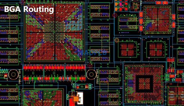
BGA Routing
Vias add flexibility to the PCB design process and complexity to the PCB fabrication and assembly process. Just as there are tolerance considerations, placement restrictions and best design practices for components and traces, so too for multilayer routing BGA connections and using vias. By applying BGA routing best practice, you can ensure that your PCB boards are less susceptible to common challenges that can impact manufacturability and functionality.
BGA Routing Challenges
BGA routing presents unique challenges that must be considered as you design your printed circuit board. The most significant of these involve ensuring the signal integrity, manufacturability and reliability of your board.
- Signal Integrity: A key signal integrity issues is impedance control, which affects transmission and reflections. The impedance can be controlled by matching trace widths between forward and return lines, using the appropriate dielectric thickness and installing a reference plane between signal layers. Installing reference or ground planes between adjacent signal traces is also effective in minimizing crosstalk. When the signals are on the same layer, maintaining the spacing between traces is key. Check SI Analysis.
- Manufacturability: In addition to determining the number of layers (signal and reference) to optimize signal integrity, you need to consider the manufacturability of the BGA scheme. There are specific restrictions and guidelines depending on how the BGA connections are routed with each other and externally. The number of layers, pitch angles, via sizes, type of hole drilling and other concerns are limited by the capabilities of the PCB board manufacturer.
- Reliability: The reliability of your PCB board depends on board construction quality and synchronization of your design with the capabilities of your PCB manufacturer by employing good DFM (design for manufacturability) practices. Not synchronize or push the limits too far can result in PCB boards that don’t function as designed or may fail at some point once deployed in the field. Copper weight, solder mask thickness, coverlay thickness, and copper grain structure are material issues that cause failure in the field. Trace routing, including via choices, may also affect operation, leading to significant costs for recalls and replacement. Applying DFM check at MADPCB that incorporates these considerations on boards that include BGAs will align your PCB design with your board manufacturer’s capabilities. Let’s take a look at the options available along with BGA routing guidelines for vias that, if employed, will enhance the signal integrity and PCB manufacturability of your board.
- BGA Via Options: The first step when designing your BGA routing scheme is to determine the number of signal layers required based upon your signal integrity considerations. A good rule of thumb is to use the equation: Number of Layers = Signals / (Routing Channels x Routing Per Channel). Remember to include reference planes when needed. With the quick-turn PCB design process, you can have your PCB layers up to 30 layers thick in a matter of days. The next step is to determine how to route your BGA signals. A number of options are available to you, but before settling on a strategy, you should consider how each may impact your PCB design:
- Through Hole Via: The most conventional method of connection through vias is through hole routing, which extends through the entire PCB board. Through-hole vias provide good signal integrity and are easy to implement but they require the most space.
- Blind Vias: For routing directly from the BGA, blind vias are the alternative to through-hole. They offer the advantage of being able to incorporate stacked vias, staggered vias or a combination of these. Stacked vias allow for a denser design; however, staggered vias do not require the precise alignment that stacked vias do. From a PCB fabrication standpoint, the relaxed tolerances make it simpler to implement staggered vias. Finally, you need to determine whether to use via-in-pad routing or dog bone routing. There are tradeoffs in complexity and space that must be considered:
- Via-in-Pad Routing: The space requirements of through-hole vias can be minimized by using via-in-pad routing. For through-hole vias, the footprint is small and routing is easy, but the PCB design is complex. Blind vias, which improve signal integrity, present the tradeoff of being difficult to route. The steps necessary to implement standard via-in-pad add significant time to the PCB manufacturing and assembly process. This can double or even triple the manufacturing turnaround time. When using via-in-pad routing, minimum via hole and pad sizes are used to save space. Due to the precision needed, this may cause breakout. Breakout is when the via extends outside of the pad. This may be a significant issue if the breakout occurs in the direction of an incoming trace to the pad. In those cases, signal integrity loss may occur. An alternative to avoid this is dog bone routing.
- Dog bone Routing: In this style of BGA routing, the via is offset from the pad and connected by a short trace, thus making a “dog bone” like shape. Dog bone routing does not need to be filled and capped process steps needed for via-in-pad routing, so it is less complex and faster to manufacture as opposed to via-in-pad. If the BGA pitch spacing allows it then this style of routing may be a better option than via-in-pad. However, designs can be complex and it can sometimes be unclear which style of via is appropriate. This is where the PCB design team of MADPCB can help. Your choice for BGA rouging may significantly affect the signal integrity and manufacturability of your PCB design. Additionally, your selection may add days to your board manufacturing turnaround time. By implementing BGA routing guidelines and best practices, you can ensure the manufacturability of your PCB board and reduce manufacturing time for your printed circuit boards.
MADPCB can help you incorporate these BGA routing best practices into your PCB design. As a electronic manufacturing service provider, PCB and assembly manufacturer, MADPCB knows better than other suppliers in cost reduction, manufacturability, reliability and turnaround considerations. Find a one-stop PCB solutions provider in your present or next PCB design, fabrication and assembly project? No search more, but MADPCB.