What Is Ground Plane in PCB?
The Ground Plane in printed circuit board (PCB) is a large area or layer of metal, like copper foil or constantan, connected to the circuit’s ground. Often designated as a VCC in PCB design. This area of metal is sometimes only a small portion of the board, or in a multilayer design, it is often a separate layer covering the entire board. Depending on the needs of the design, it may even occupy multiple layers.
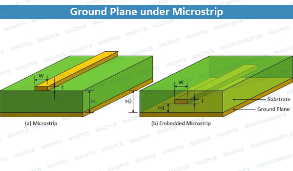
PCB Ground Plane under Microstrip
A ground plane is often made as large as possible, covering most of the area of the PCB which is not occupied by circuit traces. Similar to how the plane is connected to the ground connection of the power supply. It’s for steady supply of voltage to your board. Whenever a component needs to draw power, simply run a trace to a via that makes contact with the power plane and completes your circuit.
As you notice, power planes are generally seen in rigid board design with 4 or more layers. This is because the best practice for rigid board stack-ups is to use an even number of layers. Odd layer stack-ups don’t bring any cost savings, and the resulting asymmetry can lead to warping, twisting, and other structural defects. But for flex- and rigid-flex circuits, they are generally seen in 3- or more layers.
3 Main Purposes
The ground plane intends to three main purposes in a printed circuit board:
- Voltage return: Most every component on the PCB will connect to a power net, and then the return voltage will come back through the ground net. On boards with only one or two layers, ground nets usually have to be routed in wider traces. By devoting an entire layer to the ground plane in a multi-layer board however, it simplifies connecting each component to the ground net.
- Signal return: Regular signals also need to return, and with high-speed designs it is very important that they have a clear return path on the ground planes. Without this clear return path, these signals can generate a lot of interference for the rest of the PCB.
- Reduce noise and interference: As signal speeds increase, there are more digital circuits switching states. This creates noise pulses through the ground circuit that may affect other parts of the circuit. A ground plane with its large conducting area helps reduce the amount of this disturbance because it has a lower impedance than if the ground net is routed through a trace.
By carefully planning out the layer stack-up configuration of a multi-layer circuit board, the PCB designer can use ground planes to help control the electrical performance of the board. By using a ground plane between two active signal layers, the crosstalk between the signals on those layers can be eliminated. And by making sure that there is an uninterrupted signal return path on the ground plane, the signal integrity of high-speed transmission lines can be improved. Ground planes are also connected to components that get hot in order to help dissipate the heat. See Thermal Vias, Thermal Pad and Thermal Relief.
Importance Elements of a Power Plane or a Ground Plane
A ground plane can either be a designated area of metal on a circuit board layer, or it could take up the entire layer itself. How this is done depends on the type of PCB design CAM system that you are using. Most CAD systems give you the ability to draw a plane so that it appears as a solid patch of metal, and you can designate any net for a plane whether it is ground, power, or something different. CAD systems used to use negative image planes, as that took less computing power, but most PCB designers prefer drawing positive planes today as the tools now have plenty of power for this.
The PCB designer will draw the area for the power or ground plane on the designated layer in the shape that they desire. On an inner layer of the board this is usually the entire layer, while on the exterior layers of the board it is often smaller areas to service specific components or group of components. In some cases, the designer may split the plane on an inner layer. This can prove to be very useful when cutting back on how many layers the board will be made with. Usually, a plane split is done for power nets however, while the ground plane remains a full copper layer to help improve signal integrity ad eliminate noise and interference.
When the plane is drawn by the PCB designer, the CAD tools will automatically create a connection for the component pins that are within the contours of the plane. This connection is either a thermal relief, or a direct connection (flood). Thermal reliefs are small voids in the plane around perimeter of hole used for a thru-hole pin. Without a thermal relief, the thru-hole pin would be directly connected to the plane which would act as a huge heat sink making soldering difficult. With the relief however, the part can be soldered and unsoldered much easier. All other holes, such as vias, will normally have a direct connection to the plane.
How to Effectively Create a Plane
The key to creating a good ground plane in your PCB design is to put the tools to work for you. Make sure that you go through and set up of your design rules and constraints before you start working with plane layers. Most PCB design tools will allow you to set up different connection parameters depending on the net, and the layer where the connection will be made. The rules and constraints of the PCB design system will also give plenty of flexibility in what kind of clearances that you specify. This will also help you when you are creating your ground planes as the tools will do the work for you, all you have to do is to tell is where you want your plane.
Another thin that will help you when you work with planes is to first make sure that your board layer stack-up is fully set up. This way the positioning of your plane layers will already be decided, and you won’t have to worry about changing the location and shape of your planes later on during the design.