What’s Thermal Pad in PCB?
A Thermal Pad, also called Thermal Relief Pad, or simply Thermal, which is a PCB pad connected to a copper pour using a thermal connection. It looks like a normal pad with copper “spokes” (tracks) connecting it to the surrounding copper. This prevents an outflow of heat to the attached copper surface while soldering component, and therefore negative effects to the soldering process.
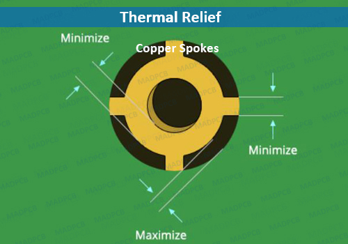
Thermal Relief
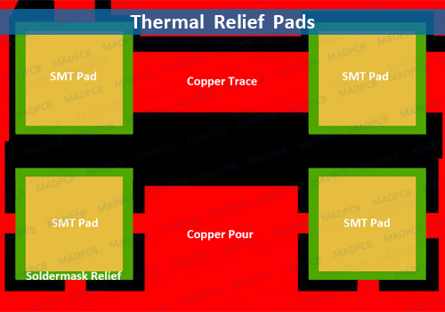
Thermal Relief Pads
A typical thermal pad on a bare board is only connected to a few narrow tracks. A pad directly connected to the copper pour is difficult to solder, since the heat quickly leaks away from the pad into the copper pour due to high thermal conductivity of copper. A thermal connection restricts the heat flow, making the pad easier to solder. Via holes that only connect one layer to another, without having soldering wires or pins into the hole, do not normally need thermal restriction.
Wire-leaded components may require the thermal relief pattern to be customized or even omitted when carrying radio-frequency currents (where the additional inductance would be problematic), or where very high current densities are expected (where the spokes of the thermal relief may act as a fuse). In these cases, the parts may require additional hand soldering during PCB assembly.
Advantages and Disadvantages
- The application of a thermal relief pad is a relatively clean process and not messy.
- The material is easy to work with and can be cut to precise sizes.
- Thermal relief pads are available in a wide range of materials allowing for custom applications.
- These are more expensive, and cutting and fitting them will add to your PCB manufacturing time.
PCB Thermal Relief in Thermal Management
Thermal relief for a PCB comes in the form of a thermal (relief) pad. These pads are connected to a copper pour using a thermal connection. Whether your PCB design is a simple single-sided or multilayer board, there will usually be some significant areas of metal on it for power conduction and ground. The metal can be a network of traces, or maybe a sizable, filled power plane.
In either case, the additional metal will behave like a heat sink for the connected pin, thus producing soldering issues such as:
- In regards to SMT component pins, these issues typically arise with smaller SMT components when soldering one of their pins directly to a large area of metal. This imbalance in the metal between the pins creates a tombstone effect, which is the result of the solder melting faster on one side than the other.
- In the case of thru-hole components, their pins can suffer from inadequate heat levels to support proper soldering, which can result in a cold solder joint. Furthermore, attempting to unsolder thru-hole components directly soldered to significant areas of metal will result in the application of excessive heat, resulting in possible PCB, trace, and component damage.
Thermal management of your PCB involves several aspects, such as the design of ground planes, trace routing, via placement, and thermal relief pads. Mastering these aspects as a PCB designer will ensure a more efficient and reliable PCB design.