What’s Copper Pour in PCB?
Copper Pour (or Copper Pouring) in PCB is an area, on a bare board filled with copper, used to make connections in printed circuit boards. Copper pour is commonly used to create a ground plane. Another reason for using it is to reduce the amount of etching fluid used during PCB manufacturing.
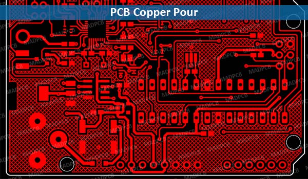
PCB Copper Pour
Copper Pours and Ground Pours
In order to accurately distinguish between copper pours and the more specific ground pours, a couple of definition may be helpful.
- Copper Pour: an area of a PCB layer that is filled with copper. The layer may be the top, bottom or any internal to the PCB stack-up and the pour may be used as a ground, reference or to isolate specific components or circuitry from the rest of the elements of the layer. Additionally, copper pours with vias can be used to aid in thermal dissipation.
- Ground Plane: an internal layer of the board stack-up that is completely filled with copper and used as a signal or power ground or reference.
- Ground Pour: a copper pour that is used for grounding and does not occupy an entire layer.
From these definitions, a ground pour can be viewed as performing a similar function to a ground plane, but occupying less area or space. Now, let’s see why and when it ca be advantageous to include PCB ground pours in your PCB design.
When and Why to Adopt a PCB Ground Pour?
Nowadays, multilayer PCB designs are more common. The reasons for this are many; including the ability to accommodate circuitry with higher complexity, flexibility to be installed in smaller, more compact products and more durable and reliable construction. Along with the use of more layers came the use of ground planes and in many cases ground pours were no longer needed to provide a reference for signals. However, there are still times when ground pours can be used to your design’s advantage, as listed below.
- Grounding on two-layer PCBs: both layers are used for signals and there is no ground plane. For these boards, ground pours can be very helpful for efficient routing by providing a central ground.
- EMI shielding: For a good multilayer design, it is desirable to have a ground plane between two signal layers to minimize noise. If there are internal signal layers next to the surface signal layers, ground pours can help with noise reduction by adding shielding.
- Heat Sinking: Ground pours can also be used to draw heat away from high power components. Thermal vias can then be used to remove the excess heat from the board.
- Copper Balance: PCB ground pours can also your contract manufacturer (CM) during PCB assembly by balancing the amount of copper of both sides of the board. This reduces the possibility that warping may occur during reflow. In this case, cross-hatching may be a better alternative to solid copper ground pours.
- High current paths: It can be advantageous to add surface ground pours to provide a short return path for high current devices; such as switching converters, instead running longer traces to a ground plane.
PCB ground pours are sometimes used, wrongly, simply to fill in the unused space on a board. Although this is not a good reason for ground pours, there are times when they should be utilized as listed above.