What Are Thermal Vias?
Thermal Vias are simple plated through holes (PTHs) that located under a surface-mounted heat source component in a printed circuit board (PCB) that allow heat transfer. The vias establish a low thermal resistance path from the top copper to the bottom side of the PCB. While, only one via cannot dissipate heat well, and generally requires vias Array.
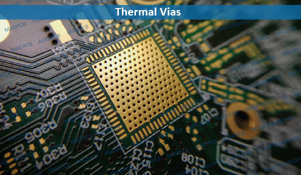
Thermal Vias
Also see terms: Thermal Pad, Thermal Relief
Heatsink and Thermal Vias Array Combination
When going to a power device example, copper planes in the PCB work as heat spreaders, and establish the horizontal thermal conduction. In traditional PCB design, designers always add a heatsink attached to the bottom copper plane under the power device to dissipate heat away from the circuit board. But when strategically add an array of thermal vias as vertical conduction through the board, it would be the best method to dissipate heat.
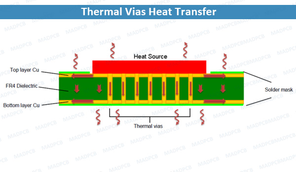
Thermal Vias Heat Transfer
Where and How to Place Thermal Vias Array?
To improve heat dissipation, the through-hole contacts should have an increased copper layer thickness. While you can use different diameters for vias, the optimal final diameter for the best thermal conductivity is 0.30 millimeters. The optimal distance from via-to-via is 0.80 mm.
Before vias array placement, it’s better to confirm the via-to-via distance first, and the gaps are dependent on different heat source components. Then consider where to place -the vias are placed directly below the heat-dissipating plate on the bottom surface of the package. In cases where heat dissipation is insufficient using only vias directly below the bottom heat-dissipating plate, vias are also placed on the periphery of the IC. In this case also, it is important that the vias be positioned as close to the IC as possible.
All setup related to the array, including via diameter, quantity, shape and other parameters will probably differ depending on the expertise at different companies, and may be formulated as design rules. In such cases, the above remarks should be kept in mind when researching how best get satisfactory heat dissipation.
You can use simulation tools to define the size and shape of thermal pads as well as select the best substrate materials to handle larger thermal loads. In addition, you can use simulation tools to analyze the performance of components and to identify possible hotspots on the board.
Simulations can show the heat flow from the top surface of the board and the underside copper plane and illustrate the relationship between thermal resistance and the number of vias.
Via-in-Pad
Simple vias or via-in-pad can play the role of thermal vias, and can provide a large reduction in thermal resistance. You can also place filled and capped vias directly under the thermal solder pad for circuit board applications that have a thickness greater than 0.70 millimeters. Filling a via with epoxy and capping it with copper prevents the solder flow from any uncontrolled solder flow. In addition, filled and capped vias ensure excellent soldering.
Simple vias or via-in-pad can provide a large reduction in thermal resistance. You can also place filled and capped vias directly under the thermal solder pad for circuit board applications that have a thickness greater than 0.70 millimeters. Filling a via with epoxy and capping it with copper prevents the solder flow from any uncontrolled solder flow.