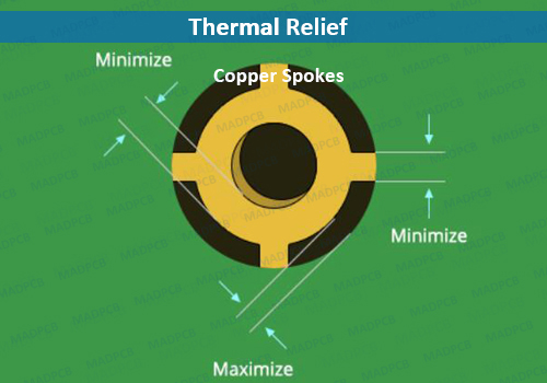
A Thermal Relief or Heat Relief is a type of circuit pad used at a location where there is a component pin or fan-out via that connects to a copper plane. The pad of a thermal relief is connected to the copper pour through 3 to 4 traces or spokes. Also see Thermal Vias.
Thermal Relief
Thermal relief is a technique used by PCB manufacturers to thermally separate soldering pads from large copper areas, to prevent excessive heat transfer from the pads during the soldering process, which would result in delayed melting of the soldering alloy or even no melting at all.
Thermal Relief Pads
Copper has high thermal conductivity. If without thermal relief design, the pin holes directly connect to the copper pour. When soldering pins to the holes, the thermal is easy to be dissipated, and hard to achieve enough thermal to melt the solder. Then the pin soldering will be harder. If with thermal relief, the pin holes keep electrical connection as well as lower thermal dissipation, then the pin soldering will be easier.
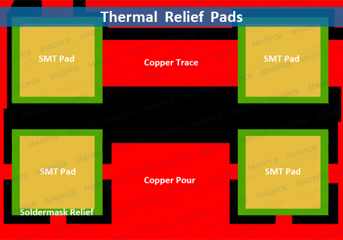
- Thru-hole component pins: These pins may not get enough heat to solder correctly, resulting in a cold solder joint. Additionally, trying to unsolder a thru-hole that is soldered directly to large areas of metal could force too much heat to be applied to melt the solder. This excess heat could potentially damage nearby traces or components.
- Surface mount component pins: Smaller two-pinned SMT parts may also have problems if one of their pins is trying to solder directly to a large area of metal. The unbalanced metal between the pins could result in the solder melting faster on one side than the other, pulling the part up and away from the other pin.
As known, thermal relief is a technique used to separate soldering pads or plated through-hole vias from large copper planes in order to reduce soldering dwell time by providing thermal resistance during the process, thus minimizing the heat transfer to the plane. However, during normal operation, the same thermal resistance limits the heat transfer for power component dissipation. The narrower the thermal pad, the greater temperature increasing during power dissipation. Hence, the dimensions of the thermal pads are critical. The work presents the results of a practical approach not for a hole via or a pad for an ordinarily component connected to a large copper area, but a medium power Surface Mounting Device, SMD, using the Printed Circuit Board, PCB, as heat sink.
When design, fabricate or assemble printed circuit boards, much care need to take to figure out whether the pin holes on copper pour has relief design or not. This is vital for manufacturing success.