Table of Contents
New Features of Electronic Devices
Electronics market calls for smaller and lighter and more reliable portable electronic devices for many years and will continue. As challenges facing to electronic devices manufactures are going to be more critical, they create new, smaller housings of the integrated circuits (ICs). As a result, there are new, alternative designs of the multioutput circuit named CSP (Chip Scale Package). This construction leads to decreasing of induction and delay time of signal propagation as well as decreasing electromagnetic noise. The trends of electronic devices in this area include:
- Creating circuits housings with electric outputs situated on each four side with very small raster <0.5mm.
- Turning wire outputs into spherical contacts.
- Turning the housings with outputs situated on its circumference into outputs situated at the whole bottom side as a net with very small raster.
- Integrating a bared semiconductor structures directly on PCB using flip-chip technology.
Circuit Pattern Imaging Challenge
Under the increasing demand for miniaturization and better functionality of electronic components and devices, and the trend of smaller and denser chips, printed circuit boards (PCBs) have been shrinking in size, which drive PCB designers to design high density interconnect (HDI) boards, and put PCB manufacturers to fabricate fine-pitch circuit boards, and make sure all the circuitry is running off these smaller chips.
While, this demand brings a lot of challenges on HDI PCB manufacturing technology, especially in circuit pattern imaging. Laser Direct Imaging (LDI) for patterning enable to achieve the best imaging results for printed circuit boards with fine lines and ultra-fine lines.
What Is Laser Direct Imaging?
The interconnection complexity of HDI PCB is still growing today. Existing technologies are unable to offer acceptable solution for fine lines. But laser direct imaging technology is considered as an answer for this challenge.
In printed circuit board (PCB) manufacturing, the imaging process is what defines the copper circuit patterns. While the conventional imaging process adopts a photo-tool and UV light to transfer circuit images, LDI only uses a computer-controlled, highly focused, laser beam to directly define the circuit patterns on the PCB CCL copper layers with laser photoresist covered.
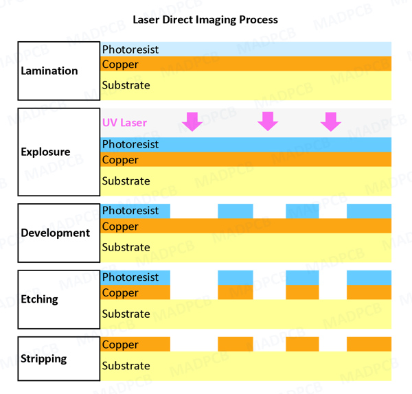
Laser Direct Imaging Process
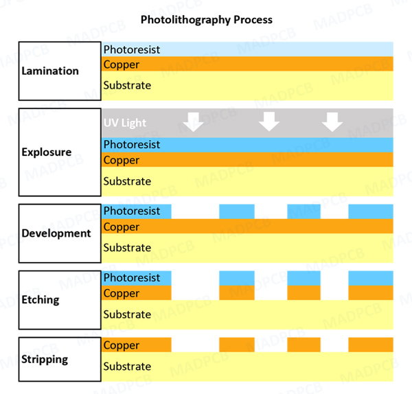
Photolithography Process
Laser Direct Imaging is the evolution of the PCB photolithography process. LDI does not adopt photo tool, but directly exposes the patterns of Gerber file onto the photoresist film. This UV photoresist is selectively exposed to the UV laser beam in increments across the laminate in a raster manner. The image formed can be compared to the image on computer screen, formed from several lines across the screen. Similar to photolithography, LDI adopts a photo-resist, although the resist is specially created for laser printing as LDI resist is fast-acting compared to conventional photo-resist. LDI resist comes in dry film and liquid options with resist application methods being identical to those used in photolithography.
Why LDI Technology?
LDI is carried out with a laser beam that is scanned across UV photoresist surface and switched on and off by means of a computer control system according to the copper circuit pattern. It has been proved that LDI systems, which work in UV spectrum are most suitable for obtaining fine lines and spaces below 0.075mm (3mil).
Traditional photolithography imaging process requires multiple steps to create the photo tool used to generate the image on the PCB. This has generated a number or challenges for PCB fabricators over the years. LDI provides a number of advantages:
- Quality: Photo film issues in the past have resulted in imperfect images due to inherent susceptibility to fluctuations in temperature or humidity. Laser imaging result in much more precision and consistent imaging, and eliminate any film-related defects.
- Laser imaging provides precision positioning and improved resolution. Image trace widths, spaces, and alignment are more accurate.
- Photo methodology requires temperature- and humidity-controlled environments to provide the most accurate transfer of images to boards. LDI reduces the impact of environment on the resulting images, and removes the impact of light reflection inherent with photo processing techniques.
In order to be used in HDI board production, an LDI system should have the following capabilities:
- High quality exposure of fine lines and spaces down to at least 0.075mm (4mil) and below of possible.
- Good depth of focus ensuring imaging quality for high topography design. This is especially needed for uniform exposure of outer layers and Sequential Build Up (SBU)
- A system design that can accommodate various product types, materials, thicknesses, manufacturing technologies and fabrication process.
- A flexible, highly accurate registration system compatible with different manufacturing technologies and production steps.
- An ability to compensate dynamically for material dimension changes in order to overcome variance in panels form the same batch and to be able to achieve tight registration tolerance over the whole area of PCB panels.
When Opt to LDI Technology?
Existing technologies are unable to offer acceptable solution and the inevitable results is reduced PCB production efficiency and lower yields. Nowadays, an average PCB trace width reaches 0.075mm (3mil) in complex multilayer PCBs. While photolithography imaging process unfortunately reached its limits due to creating high density interconnects on PCB. It is unable to creating PCB below 0.127/0.127mm (5/5mil) of trace widths and spaces. So, when most of the trace widths and spaces on a circuit board are smaller than 0.127/0.127mm (5/5mil), LDI is the best imaging option.
LDI technology is mainly used in HDI board manufacturing before. But now PCB manufacturers have to manufacture fine-line and ultra-fine-line conventional rigid, flex and rigid-flex PCBs with LDI technology where the trace widths and spaces of the conductive circuits are 0.075/0.075mm (3/3mil) or even 0.05/0.05mm (2/2mil). That’s because Laser Direct Imaging (LDI) has proved itself as the best and most comprehensive imaging solution for fine trace widths and spaces.
When portable equipment becomes more powerful also complexity of the traces on circuit board is growing. The newest trend in PCB manufacturing is multilayered PCBs. This allows to simplify all architecture of connections on motherboard. This is one of the solutions for high densities of interconnects and CSP technologies.