What is an Integrated Circuit?
An Integrated Circuit (IC), also referred to as a Chip, or a Microchip, is a set of electronic circuits on one small flat piece (or “chip”) of semiconductor material, usually silicon. Large numbers of tiny MOSFETs integrate into a small chip. This results in circuits that are orders of magnitude smaller, faster, and less expensive than those constructed of discrete electronic components. ICs are not used in virtually all electronic equipment and have revolutionized the world of electronics.
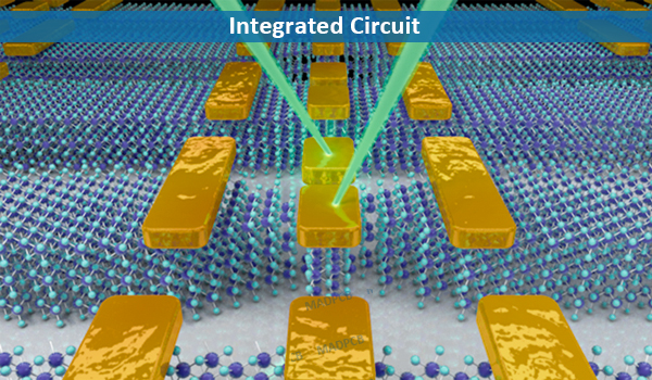
Integrated Circuit
Integrated circuits were made practical by technological advancements in metal–oxide–silicon (MOS) semiconductor device fabrication. Since their origins in the 1960s, the size, speed, and capacity of chips have progressed enormously, driven by technical advances that fit more and more MOS transistors on chips of the same size – a modern chip may have many billions of MOS transistors in an area the size of a human fingernail. These advances, roughly following Moore’s law, make computer chips of today possess millions of times the capacity and thousands of times the speed of the computer chips of the early 1970s.
ICs have two main advantages over discrete circuits: cost and performance. Cost is low because the chips, with all their components, are printed as a unit by photolithography rather than being constructed one transistor at a time. Furthermore, packaged ICs use much less material than discrete circuits. Performance is high because the IC’s components switch quickly and consume comparatively little power because of their small size and proximity. The main disadvantage of ICs is the high cost to design them and fabricate the required photomasks. This high initial cost means ICs are only commercially viable when high production volumes are anticipated.
Types
Integrated circuits can be classified into analog, digital and mixed signal, consisting of analog and digital signaling on the same IC.
Digital integrated circuits can contain billions of logic gates, flip-flops, multiplexers, and other circuits in a few square millimeters. The small size of these circuits allows high speed, low power dissipation, and reduced manufacturing cost compared with board-level integration. These digital ICs, typically microprocessors, DSPs, and microcontrollers, use boolean algebra to process “one” and “zero” signals.
Among the most advanced integrated circuits are the microprocessors or “cores”, used in personal computers, cell-phones, microwave ovens, etc. Digital memory chips, like DRAM, SRAM, EPROM, PROM; and application-specific integrated circuits (ASICs) are examples of other families of integrated circuits.
In the 1980s, programmable logic devices were developed. These devices contain circuits whose logical function and connectivity can be programmed by the user, rather than being fixed by the integrated circuit manufacturer. This allows a chip to be programmed to do various LSI-type functions such as logic gates, adders and registers. Programmability comes in various forms – devices that can be programmed only once, devices that can be erased and then re-programmed using UV light, devices that can be (re)programmed using flash memory, and field-programmable gate arrays (FPGAs) which can be programmed at any time, including during operation. Current FPGAs can (as of 2016) implement the equivalent of millions of gates and operate at frequencies up to 1 GHz.
Analog ICs, such as sensors, power management circuits, and operational amplifiers (op-amps), process continuous signals, and perform analog functions such as amplification, active filtering, demodulation, and mixing.
ICs can combine analog and digital circuits on a chip to create functions such as analog-to-digital converters and digital-to-analog converters. Such mixed-signal circuits offer smaller size and lower cost, but must account for signal interference. Prior to the late 1990s, radios could not be fabricated in the same low-cost CMOS processes as microprocessors. But since 1998, radio chips have been developed using RF CMOS processes. Examples include DECT cordless phone, or 802.11 (Wi-Fi) chips.
Modern electronic component distributors often further sub-categorize integrated circuits:
- Digital ICs are categorized as logic ICs (such as microprocessors and microcontrollers), memory chips (such as MOS memory and floating-gate memory), interface ICs (level shifters, serializer/deserializer, etc.), power management ICs, and programmable devices.
- Analog ICs are categorized as linear integrated circuits and RF circuits (radio frequency circuits).
- Mixed-signal ICs are categorized as data acquisition ICs (including A/D converters, D/A converters, digital potentiometers), clock/timing ICs, switched capacitor (SC) circuits, and RF CMOS circuits.
- 3D ICs are categorized into through-silicon via (TSV) ICs and Cu-Cu connection ICs.
Packaging of Integrated Circuits
The earliest integrated circuits were packaged in ceramic flat packs, which continued to be used by the military for their reliability and small size for many years. Commercial circuit packaging quickly moved to the dual in-line package (DIP), first in ceramic and later in plastic, which is commonly cresol-formaldehyde-novolac. In the 1980s pin counts of VLSI circuits exceeded the practical limit for DIP packaging, leading to pin grid array (PGA) and leadless chip carrier (LCC) packages. Surface mount packaging appeared in the early 1980s and became popular in the late 1980s, using finer lead pitch with leads formed as either gull-wing or J-lead, as exemplified by the small-outline integrated circuit (SOIC) package – a carrier which occupies an area about 30–50% less than an equivalent DIP and is typically 70% thinner. This package has “gull wing” leads protruding from the two long sides and a lead spacing of 0.050 inches.
In the late 1990s, plastic quad flat pack (PQFP) and thin small-outline package (TSOP) packages became the most common for high pin count devices, though PGA packages are still used for high-end microprocessors.
Ball grid array (BGA) packages have existed since the 1970s. Flip-chip Ball Grid Array packages, which allow for a much higher pin count than other package types, were developed in the 1990s. In an FCBGA package, the die is mounted upside-down (flipped) and connects to the package balls via a package substrate that is similar to a printed circuit board (PCB) rather than by wires. FCBGA packages allow an array of input-output signals (called Area-I/O) to be distributed over the entire die rather than being confined to the die periphery. BGA devices have the advantage of not needing a dedicated socket but are much harder to replace in case of device failure.
Intel transitioned away from PGA to land grid array (LGA) and BGA beginning in 2004, with the last PGA socket released in 2014 for mobile platforms. As of 2018, AMD uses PGA packages on mainstream desktop processors, BGA packages on mobile processors, and high-end desktop and server microprocessors use LGA packages.
Electrical signals leaving the die must pass through the material electrically connecting the die to the package, through the conductive traces (paths) in the package, through the leads connecting the package to the conductive traces on the printed circuit board. The materials and structures used in the path these electrical signals must travel have very different electrical properties, compared to those that travel to different parts of the same die. As a result, they require special design techniques to ensure the signals are not corrupted, and much more electric power than signals confined to the die itself.
When multiple dies are put in one package, the result is a system in package, abbreviated SiP. A multi-chip module (MCM), is created by combining multiple dies on a small substrate often made of ceramic. The distinction between a large MCM and a small printed circuit board is sometimes fuzzy.
Generations of Integrated Circuit
In the early days of simple integrated circuits, the technology’s large scale limited each chip to only a few transistors, and the low degree of integration meant the design process was relatively simple. Manufacturing yields were also quite low by today’s standards. As metal–oxide–semiconductor (MOS) technology progressed, millions and then billions of MOS transistors could be placed on one chip, and good designs required thorough planning, giving rise to the field of electronic design automation, or EDA. Some SSI and MSI chips, like discrete transistors, are still mass-produced, both to maintain old equipment and build new devices that require only a few gates. The 7400 series of TTL chips, for example, has become a de facto standard and remains in production.
| Acronym | Name | Year | Transistor count | Logic gates number |
| SSI | small-scale integration | 1964 | 1 to 10 | 1 to 12 |
| MSI | medium-scale integration | 1968 | 10 to 500 | 13 to 99 |
| LSI | large-scale integration | 1971 | 500 to 20 000 | 100 to 9999 |
| VLSI | very large-scale integration | 1980 | 20 000 to 1 000 000 | 10 000 to 99 999 |
| ULSI | ultra-large-scale integration | 1984 | 1 000 000 and more | 100 000 and more |
Small-scale integration (SSI)
The first integrated circuits contained only a few transistors. Early digital circuits containing tens of transistors provided a few logic gates, and early linear ICs, such as the Plessey SL201 or the Philips TAA320 had as few as two transistors. The number of transistors in an integrated circuit has increased dramatically since then. The term “large scale integration” (LSI) was first used by IBM scientist Rolf Landauer when describing the theoretical concept; that term gave rise to the terms “small-scale integration” (SSI), “medium-scale integration” (MSI), “very-large-scale integration” (VLSI), and “ultra-large-scale integration” (ULSI). The early integrated circuits were SSI.
SSI circuits were crucial to early aerospace projects, and aerospace projects helped inspire development of the technology. Both the Minuteman missile and Apollo program needed lightweight digital computers for their inertial guidance systems. Although the Apollo Guidance Computer led and motivated integrated-circuit technology, it was the Minuteman missile that forced it into mass-production. The Minuteman missile program and various other United States Navy programs accounted for the total $4 million integrated circuit market in 1962, and by 1968, U.S. Government spending on space and defense still accounted for 37% of the $312 million total production.
The demand by the U.S. Government supported the nascent integrated circuit market until costs fell enough to allow IC firms to penetrate the industrial market and eventually the consumer market. The average price per integrated circuit dropped from $50.00 in 1962 to $2.33 in 1968. Integrated circuits began to appear in consumer products by the turn of the 1970s decade. A typical application was FM inter-carrier sound processing in television receivers.
The first application MOS chips were small-scale integration (SSI) chips. Following Mohamed M. Atalla’s proposal of the MOS integrated circuit chip in 1960, the earliest experimental MOS chip to be fabricated was a 16-transistor chip built by Fred Heiman and Steven Hofstein at RCA in 1962. The first practical application of MOS SSI chips was for NASA satellites.
Medium-scale integration (MSI)
The next step in the development of integrated circuits introduced devices which contained hundreds of transistors on each chip, called “medium-scale integration” (MSI).
MOSFET scaling technology made it possible to build high-density chips. By 1964, MOS chips had reached higher transistor density and lower manufacturing costs than bipolar chips.
In 1964, Frank Wanlass demonstrated a single-chip 16-bit shift register he designed, with a then-incredible 120 MOS transistors on a single chip. The same year, General Microelectronics introduced the first commercial MOS integrated circuit chip, consisting of 120 p-channel MOS transistors. It was a 20-bit shift register, developed by Robert Norman and Frank Wanlass. MOS chips further increased in complexity at a rate predicted by Moore’s law, leading to chips with hundreds of MOSFETs on a chip by the late 1960s.
Large-scale integration (LSI)
Further development, driven by the same MOSFET scaling technology and economic factors, led to “large-scale integration” (LSI) by the mid-1970s, with tens of thousands of transistors per chip.
The masks used to process and manufacture SSI, MSI and early LSI and VLSI devices (such as the microprocessors of the early 1970s) were mostly created by hand, often using Rubylith-tape or similar. For large or complex ICs (such as memories or processors), this was often done by specially hired professionals in charge of circuit layout, placed under the supervision of a team of engineers, who would also, along with the circuit designers, inspect and verify the correctness and completeness of each mask.
Integrated circuits such as 1K-bit RAMs, calculator chips, and the first microprocessors, that began to be manufactured in moderate quantities in the early 1970s, had under 4,000 transistors. True LSI circuits, approaching 10,000 transistors, began to be produced around 1974, for computer main memories and second-generation microprocessors.
Very-large-scale integration (VLSI)
“Very-large-scale integration” (VLSI) is a development started with hundreds of thousands of transistors in the early 1980s, and, as of 2016, transistor counts continue to grow beyond ten billion transistors per chip.
Multiple developments were required to achieve this increased density. Manufacturers moved to smaller MOSFET design rules and cleaner fabrication facilities. The path of process improvements was summarized by the International Technology Roadmap for Semiconductors (ITRS), which has since been succeeded by the International Roadmap for Devices and Systems (IRDS). Electronic design tools improved, making it practical to finish designs in a reasonable time. The more energy-efficient CMOS replaced NMOS and PMOS, avoiding a prohibitive increase in power consumption. The complexity and density of modern VLSI devices made it no longer feasible to check the masks or do the original design by hand. Instead, engineers use EDA tools to perform most functional verification work.
In 1986, one-megabit random-access memory (RAM) chips were introduced, containing more than one million transistors. Microprocessor chips passed the million-transistor mark in 1989 and the billion-transistor mark in 2005. The trend continues largely unabated, with chips introduced in 2007 containing tens of billions of memory transistors.
ULSI, WSI, SoC and 3D-IC
To reflect further growth of the complexity, the term ULSI that stands for “ultra-large-scale integration” was proposed for chips of more than 1 million transistors.
Wafer-scale integration (WSI) is a means of building very large integrated circuits that uses an entire silicon wafer to produce a single “super-chip”. Through a combination of large size and reduced packaging, WSI could lead to dramatically reduced costs for some systems, notably massively parallel supercomputers. The name is taken from the term Very-Large-Scale Integration, the current state of the art when WSI was being developed.
A system-on-a-chip (SoC or SOC) is an integrated circuit in which all the components needed for a computer or other system are included on a single chip. The design of such a device can be complex and costly, and whilst performance benefits can be had from integrating all needed components on one die, the cost of licensing and developing a one-die machine still outweigh having separate devices. With appropriate licensing, these drawbacks are offset by lower manufacturing and assembly costs and by a greatly reduced power budget: because signals among the components are kept on-die, much less power is required (see Packaging). Further, signal sources and destinations are physically closer on die, reducing the length of wiring and therefore latency, transmission power costs and waste heat from communication between modules on the same chip. This has led to an exploration of so-called Network-on-Chip (NoC) devices, which apply system-on-chip design methodologies to digital communication networks as opposed to traditional bus architectures.
A three-dimensional integrated circuit (3D-IC) has two or more layers of active electronic components that are integrated both vertically and horizontally into a single circuit. Communication between layers uses on-die signaling, so power consumption is much lower than in equivalent separate circuits. Judicious use of short vertical wires can substantially reduce overall wire length for faster operation.
Turnkey PCB assembly with components sourcing service at MADPCB.