What is a Flip Flop?
In electronics, a Flip Flop (sometimes Flip-flop) is a circuit with two stable states that can be used to store binary data. The stored data can be changed by applying varying inputs. Flip flops and latches are fundamental building blocks of digital electronics systems used in computers, communications, and many other types of systems. Both are used as data storage elements. It is the basic storage element in sequential logic.
Differences between Flip Flop and Latch
The basic difference between them is a gating or clocking mechanism. In Simple words. Flip Flop is edge-triggered and a latch is level triggered.
Latches are something in your design that always needs attention. There are tools that help designers pinpoint the existence of latches in their design as ‘must know’ information. And then, it is the designer’s responsibility to correct if the latch usage is unintentional, as this could easily have happened due to poor RTL coding practices.
Once the latch existence is acknowledged at the synthesis level, then the downstream tools follow those conventions. This statement is suitable for ASICs, but latch existence is not acceptable for FPGAs. It would be fine to say that FPGA tools have more accurate timing analysis for the flop-based designs.
An expert designer knows how to utilize the time-borrowing capability of a latch for slack balancing while optimizing latch based critical paths in the design. Once he or she decides to use latches in a particular design, the engineer has to make sure that the enable signal is stable and valid data is being captured in the latch. This helps to avoid unstable states in the design.
Here are few differences between them for your reference below:
| Latch | Flip Flop |
| The latch is transparent – because input is directly connected to output when enable is high. It means Latch is sensitive to pulse duration (also called soft barrier) | It is a pair of latches (master and slave flop). It is sensitive to pulse transition. The signal only propagates through on the rising/falling edge (also called hard barrier) |
| Less Area (less gates) | More Area (more gates) because flip-flop contains two latches. |
| Less Power (less gates) | More Power (more gates) |
| Fast – (The longer combinational path can be compensated by shorter path delays in the subsequent logic stages. That’s why, for higher performance, circuits designer are turning to latched-based design.) |
Slow – (The delay of a combinational logic path of a design using edge-triggered flip-flops always less than the clock period except for those specified as false paths and multiple-cycle paths. Hence the longest path of a design limits the circuit performance.) |
| Require more tool manipulation and more hand-calculations to verify that they meet timing | Easy to check design timing using Static Timing Analysis (STA) tools |
| Cycle-borrowing to gain more setup time on the next register stage, as long as each loop completes in one cycle | Data launches on one rising edge, so it must set up before the next rising edge. If it arrives late, the system fails. If it arrives early, time is wasted due to hard edges in Flops |
| To meet the timing in the design, Designers consider latches to adjust timing mismatch. | |
| For ASICs with large clock skew, latches have substantial benefits for reducing the clock period | Even for the high-speed pulsed flip-flops with zero setup time, as they are not transparent, the impact of the clock skew is not reduced |
| Level-sensitive latches reduce the impact of the inaccuracy of wire load models and process variation. | Flip-flops demands for the highly accurate wire load model and process |
| In DFT, Latches needed as a lockup state at the clock domain crossings in the scan chain to avoid unpredictable behavior | In DFT, use flops that can be scanned (controllable and observable) |
| In FPGA, level-sensitive transparent latches should be avoided in FPGAs | In FPGA, edge-sensitive flip-flops are used exclusively. Timings analysis is more appropriate with flops for FPGA tools |
| Circuit analysis is complex. You may see last minutes timing mismatch surprises at the implantation stage. | Circuit analysis is easy |
| High-speed microprocessor designs typically use master-slave latches instead of flip-flops so that logic can be added between the rising and falling clock edges. | The most commonly used flop in the design world is D type flip-flop. |
| Most of these companies have written their own specialized STA tools to verify latch-based designs. | FSM implementation mostly involves D Flip-flops due to a minimum number of logic gates and lesser cost as compared to other types of flip-flops. |
| For non-timing-critical configuration registers, latches work great, due to fewer gates and less power consumption | For non-power aware design, Flip-flops are preferred over Latches |
| The latch is an asynchronous block. Therefore you must ensure that the combinational functions, which generate input signals for the latch, are race-free. Otherwise, they may generate glitches, which may be latched, causing hazards in your system. | A flip-flop, on the other hand, is edge-triggered and only changes state when a control signal goes from high to low or low to high |
| Latch based design is noisy because any noise in the enable signal disrupts the latch output easily. | Flip-flop based design is robust |
SR Flip Flop
There are majorly 4 types of flip-flops, with the most common one being SR flip-flop. This simple flip-flop circuit has a set input (S) and a reset input (R). In this system, when you Set “S” as active the output “Q” would be high and “Q‘” will be low. Once the outputs are established, the wiring of the circuit is maintained until “S” or “R” go high, or power is turned off. As shown above, it is the simplest and easiest to understand. The two outputs, as shown above, are the inverse of each other. The truth table of SR Flip-Flop is highlighted below.
|
S |
R | Q | Q’ |
| 0 | 0 | 0 |
1 |
|
0 |
1 | 0 | 1 |
| 1 | 0 | 1 |
0 |
|
1 |
1 | ∞ |
∞ |
JK Flip Flop
Due to the undefined state in the SR flip-flop, another flip-flop is required in electronics. The JK flip-flop is an improvement on the SR flip-flop where S=R=1 is not a problem.
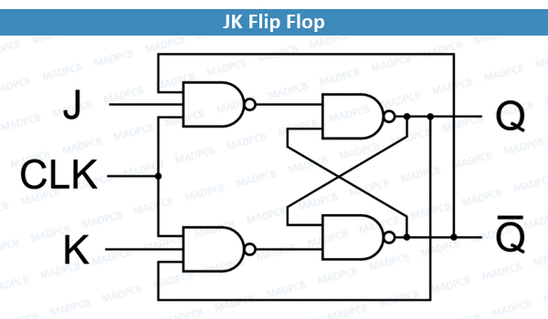
JK Flip Flop
The input condition of J=K=1, gives an output inverting the output state. However, the outputs are the same when one tests the circuit practically.
In simple words, If J and K data input are different (i.e. high and low) then the output Q takes the value of J at the next clock edge. If J and K are both low then no change occurs. If J and K are both high at the clock edge then the output will toggle from one state to the other. JK Flip-Flops can function as Set or Reset Flip-flops
|
J |
K | Q | Q’ |
| 0 | 0 | 0 |
0 |
|
0 |
1 | 0 | 0 |
| 1 | 0 | 0 |
1 |
|
1 |
1 | 0 | 1 |
| 0 | 0 | 1 |
1 |
|
0 |
1 | 1 | 0 |
| 1 | 0 | 1 |
1 |
|
1 |
1 | 1 |
0 |
D Flip Flop
D flip-flop is a better alternative that is very popular with digital electronics. They are commonly used for counters and shift-registers and input synchronization.
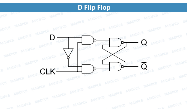
D Flip Flop
In this, the output can be only changed at the clock edge, and if the input changes at other times, the output will be unaffected.
|
Clock |
D | Q | Q’ |
| ↓ » 0 | 0 | 0 |
1 |
|
↑ » 1 |
0 | 0 |
1 |
|
↓ » 0 |
1 | 0 | 1 |
| ↑ » 1 | 1 | 1 |
0 |
The change of state of the output is dependent on the rising edge of the clock. The output (Q) is same as the input and can only change at the rising edge of the clock.
T Flip Flop
A T flip-flop is like a JK flip-flop. These are basically a single input version of JK flip-flops. This modified form of JK flip-flop is obtained by connecting both inputs J and K together. It has only one input along with the clock input.
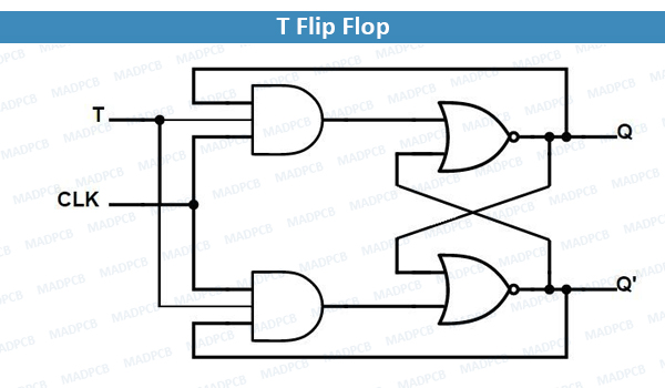
T Flip Flop
These flip-flops are called T flip-flops because of their ability to complement its state (i.e.) Toggle, hence the name Toggle flip-flop.
|
T |
Q | Q (t+1) |
| 0 | 0 |
0 |
|
1 |
0 | 1 |
| 0 | 1 |
1 |
|
1 |
1 |
0 |
Applications
These are the various types of flip-flops being used in digital electronic circuits and the applications of Flip-flops are as specified below.
- Counters
- Frequency Dividers
- Shift Registers
- Storage Registers