Table of Contents
What are Thin and Thick Film Resistors?
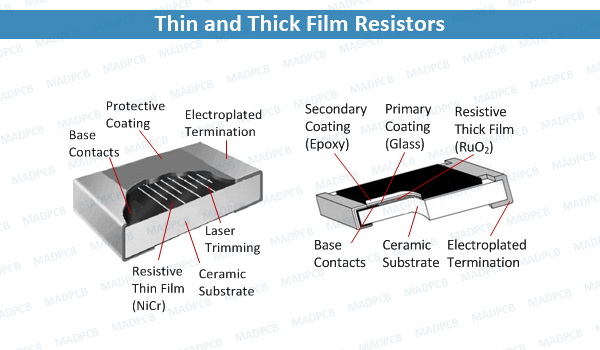
Thin and Thick Film Resistors are the most common types in the market. They are characterized by a resistive layer on a ceramic base. Although their appearance might be very similar, their properties and manufacturing process are very different. The naming originates form the different layer thicknesses. Thin film has a thickness in the order of 0.1μm or smaller, while thick film is thousands times. However, the main difference is the method used to apply the resistive film onto the substrate. Thin film resistors have a metallic film that is vacuum deposited on an insulating substrate. Thick film resistors are produced by firing a special paste onto the substrate. The paste is mixture of glass and metal oxides. Thin film is more accurate, has better temperature coefficient and is more stable. Therefore, it competes with other technologies that feature high precision, such as wirewound or bulk metal foil. On the other hand, thick film is preferred for applications where these high requirements are not critical since prices are much lower.
Thin and Thick Film Resistors
Thin Film Technology in Resistors
The resistive layer is sputtered (vacuum deposition) onto a ceramic base. This creates a uniform metallic film of around 0.1μm thick. Often an alloy of Nickel and Chromium (Nichrome) is used. Thin film resistors are produced with different layer thicknesses to accommodate a range of resistance values. The layer is dense and uniform, which makes it suitable to trim the resistance value by a subtractive process. Photo etching or laser trimming are used to create patterns in the film to increase the resistive path and to calibrate the resistance value. The base is often alumina ceramic, silicon or glass. Usually, thin film is produced as a chip or SMD resistor, but the film can also be applied onto a cylindrical base with axial leads. In this case, more often the term metal film resistor is used.
Thin film is usually used for precision applications. They feature relatively high tolerances, or temperature coefficients and low noise. Also, for high frequency application, thin film performs better than thick film. Inductance and capacitance are generally lower. The parasitic inductance of thin film can be higher if it is manufactured as a cylindrical helix (metal film resistor). The higher performance of thin film resistors comes with a cost, which can be factors higher than the prices of thick film resistors. Typical examples where thin film resistors are used include medical equipment, audio installations, precision controls and measurement devices.
Thick Film Technology
In the 1970s, thick film resistors started to gain popularity. Today, these are by far the most used resistors in electrical and electronic devices. They are usually packaged as a surface mount (SMD) chip resistor and have the lowest cos compared to any other technology.
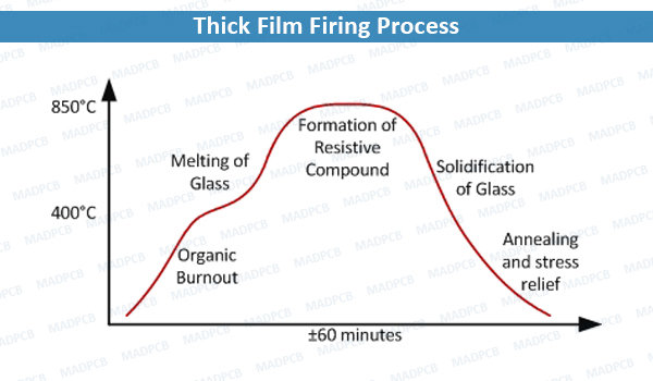
The resistive material is special paste with a mixture of a binder, a carrier, and the metal oxides to be deposited. The binder is a glassy frit and the carrier consists of organic solvent systems and plasticizers. Modern resistor pastes are based on oxides of ruthenium, iridium and rhenium. This substrate is often 95% alumina ceramic. After the firing of the paste on the carrier, the film becomes glasslike, which makes it well protected against moisture. The complete thick film firing process is schematically depicted in the graph below.
Thick Film Firing Process
The thickness is on the order of 100μm. This is approximately 1000 times more than thin film. Unlike thin film, this manufacturing process is additive. This means that the resistive layers are added sequentially to the substrate to create the conducting patterns and resistance values.
The temperature coefficient typically ranges from 50 to 200ppm/oC. Tolerances are between 1% and 5%. Because costs are low, thick film is generally preferred is applications that allow more tolerance in the resistance value, higher TCR or lower stability. Therefore, these resistors can be found in almost any device with an AC Plug or a battery. Advantages of thick over thin technology are not only lower cost, but also the ability to handle more power, provide a wider range of resistance values, and withstand high surge conditions.
Differences between Thin and Thick Film
In the table below the main differences between the two technologies are listed. The components may look the same, but the production method and the electrical properties are definitely different.
| Characteristic | Thin Film | Thick Film |
| Film Thickness (μm) | +/-0.1 | +/-100μm |
| Manufacturing Process | Sputtering (Vacuum Deposition) | Screen and stencil printing |
| Trimming | Abrasive or Laser, for complex patterns: photo etching |
Abrasive or Laser |
| Resistive Material | Uniform metallic film, usually Nichrome |
Paste of Ruthenium Oxide or other ally |
| Resistive Value (MΩ) | 0.2 ~ 20 | 1 ~ 100 |
| Tolerance (%) | +/-0.1 ~ 0.2 | +/-1 ~ 5 |
| Temperature Coefficient (ppm/oC) | +/-5 ~ 50 | +/-50 ~ 200 |
| Max Operating Temperature (oC) | 155 | 155 |
| Max Operating Voltage Umax (V) | 50-500 | 50-200 |
| Non-linearity (dB) | >110 | >50 |
| Current Noise (μV/V) | <0.1 | <10 |
| Power Rating P70 (W) | 1/16 ~ 1 | 1/16 ~ 1/4 |
| Stability at P70 (1000h) ∆R/R % | +/-0.15 ~ 0.5 | +/-1 ~ 3 |
| Moisture Resistance | Thick film is more resistant to moisture, since they are glass like. | |
| High Frequency Behavior | Thin film features lower parasitic inductance and capacitance. However, inductance may be high if thin film is manufactured with a cylindrical shape that is spiral cut. | |
| Typical Areas of Use | High Precision: Measuring Monitoring Medical Audio precision controls |
Very Wide: almost any electrical device with battery or AC connection. The average PC contains well over 1000 thick film chip resistors. |
| Cost | More expensive than thick film | Lowest cost resistor type on the market. Preferred solution if performance requirements are low. |
| Estimated Use in Analog Circuits | 20% | 80% |
Thin film and thick film technologies are used for ceramic PCB and carbon printed PCB manufacturing.