What’s Sputtering?
Sputtering, also called Sputter Deposition/Coating, is a PVD (Physical Vapor Deposition) class of Thin Film technology. The materials to be coated (the sputtering target) is bombarded with plasma ions and the removed particles enter into the gas phase. The vapor then condenses on the substrate surface, adheres to it firmly, and forms a very thin layer. This process enables the uniform application of very diverse substances (metals, alloys, oxides and nitrides) on a wide variety of substrates; from semiconductor wafers to architectural glass.
Of the various types, sputtering is one of the most economic deposition methods which is used as a standard coating technique in many industries. One of the main reasons for popularity of it is the fact that this method allows for a multitude of different materials to be deposited on a wide variety of substrates.
Sputtering in Ceramic PCB Manufacturing
The DC magnetron sputtering method developed in the 1970s achieves high speed, low temperature, and low damage. The deposition is a well-established coating method used in thin film technology for decades in a wide variety of applications. MADPCB adopts sputtering technology in ceramic PCB manufacturing, particularly by the means of the use of magnetrons. We offer special expertise in reactive and non-reactive magnetron sputtering with direct current (DC) and pulsed direct current (pulsed DC, unipolar and bipolar). The various sputtering technologies are integrated into MADPCB systems depending on the ceramic substrate materials used, the properties of the respective coatings and the deposition rates.
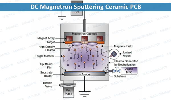
DC Magnetron Sputtering Ceramic PCB
Adding a closed magnetic field parallel to the target ceramic substrate surface in the bipolar sputtering, the secondary electron is bound to a specific area of the target surface to enhance the ionization efficiency by means of the orthogonal electromagnetic field formed on the surface of the target, increasing the ion density and energy, and finally realizing the high-rate sputtering.
Concept of Magnetron Sputtering
In a typical sputtering deposition process, a chamber is first evacuated to high vacuum to minimize the partial pressures of all background gases and potential contaminants. After base pressure has been reached, sputtering gas which comprises the plasma is flowed into the chamber and the total pressure is regulated – typically in the milliTorr range – using a pressure control system.
To initiate plasma generation, high voltage is applied between the cathode – commonly located directly behind the target – and the anode – commonly connected to the chamber as electrical ground. Electrons which are present in the sputtering gas are accelerated away from the cathode causing collisions with nearby atoms of sputtering gas. These collisions cause an electrostatic repulsion which ‘knock off’ electrons from the gas atoms, causing ionization. The positive sputter gas atoms are now accelerated towards the negatively charged cathode, leading to high energy collisions with the surface of the target. Each of these collisions can cause atoms at the surface of the target to be ejected into the vacuum environment with enough kinetic energy to reach the surface of the substrate. In order to facilitate as many high energy collisions as possible – leading to increased deposition rates – the gas is typically chosen to be a high molecular weight gas such as argon or xenon. If a reactive sputter deposition process is desired, gases such as oxygen or nitrogen can also be introduced to the chamber during film growth.