1. What Are Ceramic PCBs?
Ceramic PCB(s) are the printed circuit boards which are manufactured with ceramic (Al2O3, AlN, SiN) substrates by the means of Direct Plated Copper (DPC), Direct Bonded Copper (DBC) and Active Metal Brazing (AMB) technologies.
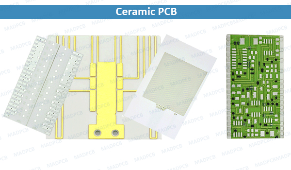
Ceramic PCB
1.1 Ceramic PCB Background
With recent advances in the market, Ceramic PCBs have become a move viable option for PCB designer. With the continuing requirements for miniaturization, microelectronics and high-power packages, the need for substrates capable of withstanding high operating temperature, whilst offering outstanding thermal performance is a must. Semiconductors from materials such as Silicon Carbide (SiC) and Gallium Nitride (GaN) operate at high temperatures meaning associated circuits need to be ceramic. Ceramic interposers are also becoming popular for thermal management and when a hermetic package is required where no moisture can be tolerated and no outgassing materials can be used.
Ceramics are also used for high frequency applications due to low signal loss and as well as resisting UV they are chemical resistant, have no outgassing and are completely water resistant.
Ceramics have been widely used in electronics/electronic components for years due to their thermal, and mechanical advantages. With recent advances in technology and manufacturing capabilities, they are now replacing entire PCBs.
Since their introduction, Ceramic PCBs have received enormous attention from the industry as an effective solution to a range of electronic issues. The superior Thermal Conductivity of ceramics with low signal loss for high frequency being the leading reasons that more and more industries are turning to ceramics for their PCB design.
1.2 Advantages Over Other Technologies
Heat dissipation is the key advantage that ceramics has over more conventional materials such as FR4 and metal core PCBs. With components being placed directly on the boards, and no isolation layer, the flow of heat through the boards is far more efficient. Depending on the material chosen, the Thermal Conductivity values range from 24-80W/m·K.
In addition to this, Ceramic material can withstand high operating temperatures (over 800°C) and has a very low CTE, allowing for additional compatibility options for PCB design.
1.3 Advantages of Ceramic Circuit Boards
- Superior values of Thermal Conductivity (up to 180W/mK)
- Higher substrate operating temperatures over 800°C
- Lower CTE
- Suitable for high-frequency applications due to low signal loss
- Possibility for Hermetic packages with 0% water absorption
2. Ceramic PCB Technologies
2.1 Direct Plated Copper (DPC)
DPC is recent development inn the field of Ceramic Substrate PCBs and was the breakthrough that made ceramics much more viable to designers. DPC involves vacuum sputtering under high temperature and pressure conditions to plate the copper to the substrate. The addition of a thin film titanium (Ti) layer acts as a bonding interface between the copper and ceramic layers. During this part of the process a very thin layer of copper is deposited coating the Ceramic substrate and it is also deposited in any pre-drilled holes. The circuit is then formed with etching. The thin copper allows very fine traces and reduced undercutting. Panels are then plated up to the required end copper thickness ranging from 10μm (≈1/3oz) to 140μm (4oz). DPC enables the circuit to incorporate plated or filled vias. Normal PTH methods do not produce reliable results on ceramics and therefore DPC must be used if a double-sided PTH ceramic board is required.
2.1.1 DPC Process Methods and Capabilities
- Direct Plated Copper (DPC) is the newest development in the field of Ceramic Substrate PCBs.
- It involves plating the copper conductor layer to the copper substrate under high temperature and pressure conditions.
- The addition of a thin titanium layer acts as a bonding interface between the copper and Ceramic layers.
- A very thin layer of Copper is deposited at this stage coating the Ceramic substrate and any pre-drilled holes.
- Track printing and etching is then performed with the thin Copper allowing for very fine tracks and reduced undercutting.
- The panels are then plated up to the required end copper thickness.
- Using this method can result in copper thickness’ ranging from 10um (≈ 1/3oz) to 140um (4oz).
- It also allows for the possibility of plated or filled vias. Something not possible with Thick Film or DBC technology.
2.1.2 DPC Ceramic PCB Applications:
- HBLED
- Substrates for solar concentrator cells
- Power semiconductor packaging including automotive motor control
- Hybrid and electric automobile power management electronics
- Packages for RF
- Microwave devices
2.2 Direct Bonded Copper (DBC)
With DBC the copper is bonded to the Ceramic substrates on one or both sides using a high-temperature oxidation process. It offers options of heavy copper thickness -140μm (4oz)-350μm (10oz). The copper and substrate are heated in an atmosphere of nitrogen containing about 30ppm of oxygen; under these conditions, a copper-oxygen eutectic forms which bonds successfully both to copper and the oxides used as substrates. With DBC the copper layers can then be etched using standard PCB technology to form required circuit. Conventional PTH processing is not suitable for ceramics and therefore only DPC is used for through hole plating.
Reminder: MADPCB now not offers Direct Bond Copper (DBC) ceramic printed circuit boards (PCBs), but offers with DPC process.
2.2.1 Ceramics -DBC Process Methods and Capabilities
- Direct Bonded Copper (DBC) is used when a high copper thickness is required – 140um (4oz)-350um (10oz). Heavy Copper.
- The copper is bonded to the Ceramic substrate on one or both sides using a high-temperature oxidation process.
- The copper and substrate are heated in an atmosphere of nitrogen containing about 30 ppm of oxygen; under these conditions, a copper-oxygen eutectic forms which bonds successfully both to copper and the oxides used as substrates.
- The copper layers can then be etched using standard PCB technology to form an electrical circuit.
- Laser drilling is then used for any through hole requirements and profile machining.
2.2.2 Disadvantages
Due to the Oxidization bonding process, there can be a slight reduction in Thermal Conductivity created by a void between the Copper and Ceramic layers.
2.2.3 Applications
Main applications are high power modules, like IGBT, CPV, or any other wide bandgap device modules.
- IGBT
- High-Frequency Switching Power Supply
- Automotive
- Aerospace
- Solar Cell Component
- Power Supply for Telecommunication
- Laser Systems
2.3 Active Metal Brazing (AMB)
AMB is the latest development in ceramic substrates. Unlike DBC Active Metal Brazing forms the substrates without metallization. Under a high temperature vacuum the copper is joined (brazed) direct to the ceramic base. This offers a high reliability substrate with unique heat dissipation. The brazing technology also enables copper weights of up to 800μm on thin ceramic substrates. These Heavy Coper materials make AMB ideal for Power Electronics.
2.3.1 Ceramics – AMB (Active Metal Brazing)
- Ceramics – AMB (Active Metal Brazing) is a new innovative way of producing Ceramic Substrates without metallisation.
- In a high temperature vacuum AMB enables copper to be joined direct to the ceramic base.
- A high reliability substrate with unique heat dissipation properties.
- Brazing technology enables copper weights of up to 800µm on thin ceramic substrates.
- Ideal for Power Electronics applications
2.3.2 AMB Single-Sided Ceramic PCB: Various copper weights are available to meet match substrate thicknesses detailed in the table below. It is recommended the copper thickness on any design is no more than half the ceramic thickness.
2.3.3 AMB Double-sided Ceramic PCB: Double sided substrates offer greater mechanical strength and stability enabling Heavy Copper to be offered on thin ceramic substrates. The following is a guide on double sided material availability although during the etching process original copper weights can be reduced.
|
Active Metal Brazing Double Sided Panels |
||||||
|
Ceramic Thickness |
Copper Thickness |
|||||
|
200µm |
250µm | 300µm | 400µm | 500µm |
800µm |
|
|
0.25mm |
SiN | SiN | SiN | SiN | SiN |
SiN |
|
AlN |
AlN |
|||||
|
0.32mm |
SiN | SiN | SiN | SiN | SiN | SiN |
| 0.38mm | AlN | AlN | AlN |
|
||
|
0.63mm |
AlN | AlN | AlN | AlN | AlN | |
| 1.00mm | AlN | AlN | AlN | AlN | AlN |
AlN |
3. Ceramic PCB Manufacturing Capabilities
|
Ceramic PCB Manufacturing Capabilities |
|||
|
Property |
AMD | DPC |
DBC |
|
Compatible Substrates |
AlN / SiN | Al2O3 / AlN / SiN |
Al2O3 / AlN / SiN |
|
Substrate Thickness (mm) |
0.25/0.32/0.38/0.63 /1.0 |
0.25/0.38/0.5/0.635 1.0/1.5/2.0 |
0.25/0.38/0.5/0.635 |
|
Copper Weight |
See Below | 10 – 140 |
140 – 350 |
|
Panel Sizes |
Standard: 115 x 115 |
Standard: 115 x 115 | Standard: 115 x 115 |
| Special: Up to 170 x 250 | Special: Up to 170 x 250 |
Special: Up to 170 x 250 |
|
|
Finish Options |
ENIG/ENEPIG/EPIG/Immersion Silver/Immersion Tin/OSP |
||
|
Min Trace Width |
Dependant on Cu Weight | 0.1 |
Dependant on Cu Weight |
|
Min Hole Diameter |
0.08 | 0.08 |
0.08 |
|
PTH Aspect Ratio |
N/A | 5:01 |
N/A |
Note: Through hole plating is not possible with AMB or DBC substrates.
4. Thick Film Ceramic PCB
- Thick Film technology involves the addition of layers of conductor (Copper or Silver) onto a Ceramic substrate via screen printing processes.
- Suitable for use with Al2O3/AlN and Sapphire substrates.
- A cost-effective solution with fewer manufacturing processes than other methods.
- With a conductor thickness between 7-20um it is not well suited to power electronics requiring high current capacity.
- Due to conductor application, it is also unsuitable for designs requiring fine tracks and/or plated/filled vias.
5. Ceramic PCB Substrate Options
- Al2O3 (Alumina Oxide): Most commonly 96%, this is the most standard and cost-effective option, with a Thermal Conductivity of around 24W/mK. A 99.6% option is also available.
- AlN (Aluminum Nitride): Required when Thermal Conductivity is the driver. With a TC of around 170W/mK it is the best option for highly demanding systems.
- SiN (Silicon Nitride): More resistant to shock than other substrate options, with a higher fracture toughness and bending strength. Well suited for automotive applications where structural reliability is key.
5.1 Ceramic Material Specifications
|
Property |
Unit | Al2O3 (96%) | Al2O3 (99.6%) | AlN |
SiN |
|
Thermal Conductivity |
W/mK | 24 | 29 | 180 |
85 |
|
CTE |
x 10-6/K | 6.7 | 6.8 | 4.6 |
2.6 |
| – | 9.8 | 9.9 | 9 | 9 | |
| Signal Loss | x 10-3 | 0.2 | 0.2 | 0.2 |
0.2 |
|
Light Reflectivity |
% | 70/85 | 75 | 35 | – |
| Dielectric Strength | KV/mm | ≥15 | ≥15 | ≥15 |
≥15 |
|
Rupture Strength |
Mpa | 400 | 550 | 450 |
800 |
|
Max Operating Temperature |
Unit | Al2O3 (96%) | Al2O3 (99.6%) | AlN |
SiN |
|
Substrate |
°C | 850 | 850 | 850 | 850 |
| Cu Conductor | °C | 300 | 300 | 300 |
300 |
| °C | < 300 | < 300 | < 300 | < 300 | |
| Tg | °C | 500 | 500 | 500 |
500 |
5.2 Al2O3 Alumina PCB (96% & 99.6%)
The most common material used for Ceramic PCBs is Al2O3 Alumina PCB (96%). A naturally excellent electrical insulator with strong thermal properties. The thermal conductivity of Alumina is not as high as Aluminum Nitride (AlN), however, it is still noticeably higher than the best performing Metal Core PCB (MCPCB) materials with a Thermal Conductivity in the region of 24W/m·K. Another variant of this is Al2O3 (99.6%) which has a higher Thermal Conductivity, in the region of 29W/m·K.
A high light reflectivity, along with good thermal properties makes Alumina Oxide well suited for LED applications. Whilst low values of thermal expansion and signal loss make it suitable for a range of applications including sensor module, high-frequency systems and cooling systems.
5.2.1 Advantages
- High values of Thermal Conductivity (24-29W/mK)
- High substrate operating temperatures to over 800°C
- Low CTE
- Suitable for high frequency applications due to low signal loss
- High light reflectivity
- Possibility for Hermetic packages with 0% water adsorption
5.3 AlN Aluminum Nitride PCB
If a higher thermal conductivity is required then Aluminum Nitride will be required. AlN has superior thermal conductivity; depending on options, the conductivity achieved will be between 150-170W/m·K.
This, along with a very low CTE and high operating temperatures makes AlN suitable for a variety of applications including; High power LEDs, testing, sensors, integrated circuits (ICs) and more.
5.3.1 Advantages
- Superior values of Thermal Conductivity (up to 170W/mK)
- High substrate operating temperatures to over 800°C
- Very low CTE
- Suitable for high frequency applications due to low signal loss
- Possibility for Hermetic packages with 0% water absorption
5.4 SiN Silicon Nitride PCB
|
Property |
Unit | SiN |
| Thermal Conductivity | W/mK |
85 |
|
CTE |
x 10-6/K | 2.6 |
| Dielectric Constant | – |
9 |
|
Signal Loss |
x 10-3 | 0.2 |
| Light Reflectivity | % |
– |
| KV/mm |
15 |
|
|
Rupture Strength |
Mpa |
800 |
|
Max Operating Temperature |
Unit |
SiN |
|
Substrate |
°C | 850 |
| Cu Conductor | °C |
300 |
|
Solder Mask |
°C | 100 |
| Tg | °C |
500 |
5.4.1 Advantages
- Thermal Conductivity value between Al2O3 and AlN at 85-90W/mK run at extremely high temperatures
- High substrate operating temperatures to over 800°C
- Very low CTE
- High rupture strength
- Suitable for high frequency applications due to low signal loss
- Possibility for Hermetic packages with 0% water absorption