What’s DPC (Direct Plated Copper)?
DPC (Direct Plated Copper) involves physical vapor deposition (PVD) method – Sputtering under high temperature and pressure conditions to plate the copper to substrates. DPC is the most advanced process in manufacturing ceramic substrate PCBs at MADPCB.
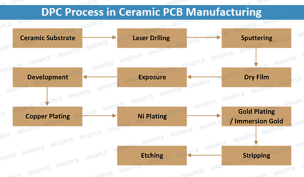
DPC Process in Ceramic PCB Manufacturing
DPC process in Ceramic PCB Manufacturing is briefly described in below figure. A simple electrical characterization for DPC substrate is then utilized to extract the high-frequency dielectric constant and dissipation factor.
DPC Process in Ceramic PCB Manufacturing
The entire DPC process basically comprises the 10 steps with details as following:
- Ceramic Substrate: There are aluminum nitride (AlN) and alumina (Al2O3) bare ceramic substrates without copper clad for choose in ceramic printed circuit board (PCB) manufacturing. We use laser to cut the ceramic substrate to the pieces board size or array size in substrate cutting step. Customers may haven’t laser machine to depaneling, so, our delivery format of ceramic PCBs are unit (single pieces) but not array (/set).
- Laser Drilling: As ceramic is fragile, holes drilling cannot be realized with mechanical NC drilling, but laser. If your board has plated through holes (PTHs), we need drilling holes through the substrate by laser. These holes can be used as via holes to communicate between both sides of the ceramic substrate if it is necessary for some specific designed board layout. NPTH drilling is also with a laser.
- Sputtering: With the sputter deposition technique, vacuum sputtering under high temperature and pressure conditions to plate the copper to the opposite sides of the bare substrate so that it is covered with a copper layer on both sides. The addition of a thin film titanium (Ti) layer acts as a bonding interface between the copper and ceramic layers. During this part of the process, a very thin copper film (generally 1μm in thickness) is deposited coating the ceramic substrate and it is also deposited in any pre-drilled holes. After sputtering process, it forms a ceramic-based copper clad laminate (CCL), i.e. DPC copper-metallized substrate.
- Dry Film: Apply dry film onto the thin copper film on both sides of the copper plated ceramic substrate.
- Exposure: A film (different from thin or thick film, but like a photo film) is made using conventional photomask technology. The photomask is flatly positioned and adheres to the dry film on the ceramic substrate, which is sent into an exposing chamber. After creating a vacuum in the exposing chamber, UV lights irradiate the dry film through the photomask, which is polymerized by the ultraviolet radiation. The dry film, which is not irradiated by the UV rays, does not react and keeps its chemical composition.
- Development: The development process etches the polymerized part of the dry film by chemical cleaning or physical cleaning. In this way, some parts of the copper film are exposed from the dry film; those parts of the copper film will form the required circuit patterns as per the Gerber artwork of the ceramic board, in order to produce the required copper areas of a circuit board on the ceramic substrate. Thus, the copper features, like patterns, annular rings and others, can be printed on the dry film.
- Copper Plating: Plating copper leads first. Then copper is deposited to fill the exposed parts of the dry film on the ceramic substrate, with suitable conductor thickness and width, by a plating technology to form the copper features. By the above processes, the metallized circuit area has slender, flat and smooth characteristics, and the heat dissipation is good. When plated copper thickness is thicker than the desired, we need to grind the extra copper off with a high-end ceramic grinding machine (same as that used in Via-in-Pad process), which has 1μm high precision per grinding cycle.
- Ni Plating: The nickel layer prevents the atoms of the copper leads diffusing into the gold layer in afterwards gold plating or immersion gold.
- Gold Plating or Immersion Gold: Nickel and gold are deposited on the upper surface of the copper. The gold layer avoids the oxidization of the conductor surface and improves the adhesion for the gold bonding wires. An optical resistance is formed on the upper surface of the copper.
- Stripping: The remaining dry on the ceramic substrate is then removed. After stripping the dry film, the copper circuit is protected by the nickel and gold layers.
- Etching: etching the seed metal copper.
Key Attributes Comparisons among DPC, Thin Film and Thick Film
Due to the DPC processes described and the materials used, several key attributes of the DPC process can be summarized as below:
- Superior CTE and high thermal conductivity
- Low electrical resistance conductor traces
- Stable up to temperature > 340°C
- Accurate feature location, compatible with automated, large format assembly
- Fine line resolution allowing high density of devices and circuitry
- Proven reliability
- Mechanically rugged ceramic construction
- Low cost, high performance ceramic solution
Below are the key attributes comparisons:
| Key Attributes | DPC | Thin Film | Thick Film |
| Conductor Electrical Conductivity | Very good. Thick copper conductor. |
Poor conductivity due to very thin film thickness. | Good conductivity. Lowered by the presence of the glass phase. |
| Via Electrical Conductivity | Very good.
Vias filled with pure copper. |
Very good. Vias filled with pure copper. |
Poor. Vias filled with 50% metal and 50% glass or pores. |
| Feature Resolution | Good. Depends on Cu thickness. |
Very good. | Good. Determined by screen print capability. |
| Cost | Low to moderate. Vias and metal deposited in the same process. |
High cost. Expensive substrate. Lapp and polish required after via deposition. |
Low to moderate. Expensive metal pastes. Low cost substrate and low cost deposition technology. |
| Thermal Performance | Very good. AIN or Al2O3 substrate and high thermal conductivity metal. |
Good. AIN or Al2O3 substrate. Metal layer too thin for heat spreading. |
Moderate. Al2O3 substrate. Conductivity through the metal is poor due to the glass phase. |
| Suitability for Power Applications | Very suitable. Copper conductors carry high currents. |
Not suitable. Thin film layers can not carry high currents. |
Suitable. Conductors with a glass phase have moderate conductivity. |
| Suitability for High Frequency Applications | Suitable. Good conductivity and line resolution |
Very suitable. Excellent line resolution. |
Not suitable |
| Green | Yes | Yes | No. Often contain Pb additives. |
Applications of DPC Metallized Substrate
Based on ceramic and thick copper construction, the DPC substrate provides outstanding thermal and electrical performance for applications in high power or high current devices. In PCB manufacturing industry, DPC technology is applicable for most of thin film Ceramic PCBs fabrication. Also see DBC.
The applications of DPC metallized substrate can be selected on high-brightness LED (HBLED), substrates for solar concentrator cells, power semiconductor packaging and automotive motor control. In addition, DPC substrates with excellent electrical performance can be considered for RF/microwave components, which require very low loss. These DPC substrates can therefore be widely used for high frequency components that require high power and high heat.