What’s Thin Film?
Thin Film refers to many technologies, which are processes for depositing and processing thin layers from a few microns thick down to individual atomic layers. The thin layer materials used as the substrate and the applications vary widely and we are surrounded by them in our daily lives: Processors and memory chips on silicon wafers for modern microelectronics, hard coatings on drill bits in PCB manufacturing, decorative iridescent layers on gemstones, anti-reflective coatings on glasses, antibacterial metal coatings on medical devices, flexible solar cells or even coatings for food packaging and medicines on miles of foil.
To be able to deposit such thin layers with well-defined characteristics, the atoms and molecules that form a layer are usually collected from the gas phase at very low pressure (vacuum) so that the concentrations can be closely controlled, as can the rate at which layers build up. When the layer is formed by condensation or re-sublimation, the process is called physical vapor deposition (PVD). In addition to the coating materials and the used method, there are many parameters that can potentially affect the final characteristics of the coating, such as the substrate temperature, the energy of the impinging particles or the chemical bonds present on the surface of the substrate.
Thin Film Ceramic PCB
In printed circuit board manufacturing, especially in Ceramic PCB, a thin film is a layer of copper deposited on the ceramic (Al2O3, AlN, SiN) substrates. The deposited copper thickness to the substrates generally is 1μm (micron). The DPC process is one of PVD processes. But the plated copper thickness cannot reach the PCB conductor’s height requirement. Next, running the thin copper layer covered ceramic substrate in traditional PCB fabrication process, then we can reach finished copper thickness as desired, ranges from 9μm (≈1/4oz) to 35μm (1oz), or even more thicker.
In microelectronic packaging, ceramic metallization is the subject of interest and has been extensively studied mechanically, chemically and electrically due to its unique properties specifically under extremely environments. How to metalize and bond copper to the ceramic substrate is the key technology to build Ceramic PCBs.
Film Deposition Technologies
The act of applying a thin film to a surface is thin-film deposition – any technique for depositing a thin film of copper onto a ceramic substrate or onto previously deposited layers. “Thin” is a relative term, but most deposition techniques control layer thickness within a few tens of nanometers. There are 3 main ceramic PCB manufacturing technologies:
- Magnetron Sputtering Copper
- Direct Plated Copper (DPC) (sputtering is included)
- Direct Bonded Copper (DBC) (eliminated by MADPCB in ceramic PCB manufacturing)
Magnetron Sputtering Copper Thin Film Process
Cu thin films are coated onto the Al2O3 substrates by DC Magnetron Sputtering using an equipment called PVD Sputter. At the beginning of the process, the chamber should be pumped to a vacuum level below 6.66x 10⁻³ Pa. With the desired background pressure, the target surface is first cleaned by argon (Ar) plasma at 50W for 5 min with the shutter closed for the following purposes:
- Removal of contaminants
- Cleaning up the oxidized surface
- Establishing an equilibrium state for the system with sufficient time.
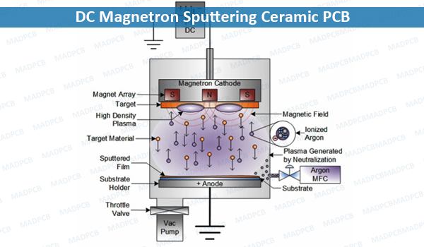
DC Magnetron Sputtering Ceramic PCB
The deposition process is conducted at a working pressure of 2.00 Pa and a DC power at 300 W. Cu sputter target is 99.99% in purity. The ceramic substrate is mounted face down, and 10 degree off axis with respect to the target. The distance for substrate-to-target is maintained at 20.0 cm. Rotation of the substrate holder is kept at 20rpm during deposition for better film uniformity. The substrate temperature is monitored by thermocouples mounted on the back of the substrate holder. Throughout this work, there is no heating applied during the film deposition unless specifically mentioned. The substrate temperature increase due to the plasma bombardment is no more than 5°C. The deposition rate of the Cu thin film under above conditions is about 0.3 nm/s.
Thin Film Copper Post-Deposition Annealing
After the Cu film was deposited, a post-deposition annealing step was performed directly inside the sputtering chamber under vacuum conditions to prevent oxidation and increase bonding adhesion strength. The annealing temperature is 300°C. The ceramic boards are heated from ambient temperature to the targeted temperatures at a heating rate of 10°C/min. After the peak temperature is reached, the boards are held at the temperature for 30min before the power is cut off. After cooling down to room temperature, the boards are removed from the chamber. The cooling rate is approximately 1°C /min.