What’s Physical Vapor Deposition (PVD)?
The term Physical Vapor Deposition (PVD), sometimes called Physical Vapor Transport (PVT), which covers specific processes used in thin film technology. In all cases, it refers to vacuum-based coating processes that use physical methods to deposit thin films on a substrate, like ceramic substrates in Ceramic PCB manufacturing.
In all PVD processes, the material from which the thin film will be produced is initially in solid form and normally located somewhere in the process chamber, e.g. at the target in sputtering. Various methods are used to vaporize the material (for example, using a short, powerful laser pulse, with an arc, or by ion or electron bombardment) which then condenses in the form of a thin film on the substrate surface.
In thermal vapor deposition, the material that produces the film is heated by an electric heater until it is released into the gas phase. Molecular beam epitaxy and ion beam sputtering deposition are also counted among the group of PVD methods. The resulting films are extremely pure and very uniform. They also adhere excellently to the substrate. PVD coatings offer an environmentally friendly alternative to the conventional electrochemical processes for many applications.
PVD describes a variety of vacuum deposition methods which can be used to produce thin films and coatings. PVD is characterized by a process in which the material goes from a condensed phase to a vapor phase and then back to a thin film condensed phase. The most common PVD processes are sputtering and evaporation. PVD is used in the manufacture of items which require thin films for mechanical, optical, chemical or electronic functions. Examples include semiconductor devices such as thin film solar panels, aluminized PET film for food packaging and balloons, and titanium nitride (TiN) (coated cutting tools for metalworking. Besides physical vapor deposition tools for fabrication, special smaller tools (mainly for scientific purposes) have been developed.
PVD Thin Film Technology: Sputtering
In thin film Ceramic PCB manufacturing, DC magnetic sputtering is a process finished in PVD or PVT line.
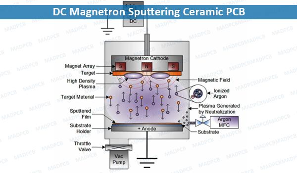
DC Magnetron Sputtering Ceramic PCB
Advantages
- PVD coatings are sometimes harder and more corrosion-resistant than coatings applied by the electroplating process. Most coatings have high temperature and good impact strength, excellent abrasion resistance and are so durable that protective topcoats are rarely necessary.
- Ability to utilize virtually any type of inorganic and some organic coating materials on an equally diverse group of substrates and surfaces using a wide variety of finishes.
- More environmentally friendly than traditional coating processes such as electroplating and painting.[citation needed]
- More than one technique can be used to deposit a given film.
Disadvantages
- Specific technologies can impose constraints; for example, the line-of-sight transfer is typical of most PVD coating techniques, however, some methods allow full coverage of complex geometries.
- Some PVD technologies typically operate at very high temperatures and vacuums, requiring special attention by operating personnel.
- Requires a cooling water system to dissipate large heat loads.