Table of Contents
PCB Copper Foil
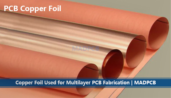
Copper (Cu) is an influential metal for both industrial and consumer applications. When it comes to PCB industry, it exists as copper foil in rolls, which can be pressed together with prepreg to the rigid or flexible copper clad laminate under heat and pressure, then to be etched into conductors of heat and electricity on conductive layers.
PCB Copper Foil
PCB Copper Weights
PCB copper foil is the initial copper thickness applied on outer and inner layers of a multilayer PCB board. Copper weight is defined as the weight (in ounces) of copper present in one square foot of area. This parameter indicates the overall thickness of copper on the layer. MADPCB utilizes the following copper weights for PCB fabrication (pre-plate). Weights measured in oz/ft2. The appropriate copper weight can be selected to fit the design requirement.
- 5oz copper (18μm or 0.7mil thick)
- 1oz copper (35μm or 1.4mil thick)
- 2oz copper (70μm or 2.8mil thick)
- Other reaches to 3oz, 4oz and 5oz
ED and RA Copper Foils
- Electro Deposited (ED) Copper: With ED copper, there is a huge diversity of foils regarding surface roughness, treatments, grain structure, etc. As a general statement, ED copper has a vertical grain structure. The standard ED copper typically has a relatively high profile or rough surface as compared to Rolled Annealed (RA) Copper. ED copper tends to lack flexibility and does not promote good signal integrity.
- Rolled Annealed (RA) Copper: RA Copper has been used extensively in the flex circuits manufacturing and rigid-flex PCB fabrication for decades. The grain structure and smooth surface is ideal for dynamic, flexible circuitry applications. Another area of interest with rolled copper types exists in the high-frequency signals and applications. It has been proven that copper surface roughness can impact high-frequency insertion loss and a smoother copper surface is advantageous.
Copper Foil Features
- In PCB manufacturing, the copper foils are in rolls, which are electronic grade with purity of 99.7%, and thickness of 1/3oz/ft2 (12μm or 0.47mil) – 2oz/ft2 (70μm or 2.8mil).
- Copper foil has lower rate of surface oxygen and can be pre-attached by laminate manufacturers to various base materials, such as metal core, polyimide, FR-4, PTFE and ceramic, to produce copper clad laminates.
- It also can be introduced in a multilayer board as copper foil itself before pressing.
- In conventional PCB manufacturing, the final copper thickness on inner layers remains of the initial copper foil; On outer layers we plate extra 18-30μm copper on the tracks during the panel plating process.
- The copper for the outer layers of multilayer boards is in the form of copper foil and pressed together with the prepregs or cores. For use with microvias in HDI PCB, the copper foil is directly on RCC (resin coated copper).
Surface Conductor Thickness (Foil Plus Plating)
Unless otherwise specified on the procurement documentation, the minimum total copper (copper foil plus copper plating) conductor thickness after processing shall in accordance with Table 3-1 in IPC-A-600G.
Table 3-1 External Conductor Thickness after Plating
| Weight | Absolute Cu Min. (IPC-4562 less 10% reduction) (μm) [μin] |
Plus Min. Plating for Class 1 & 2 (20μm) [787μin] |
Plus Min. Plating for Class 3 (25μm) [984μin] |
Max. Variable Processing Allowance Reduction* (μm) [μin] |
Min. Surface Conductor Thickness after Processing (μm)[μin] |
|
| Class 1 & 2 | Class 3 | |||||
| 1/8oz | 4.60 [181] | 24.60 [967] | 29.6 [1,165] | 1.50 [59] | 23.1 [909] | 28.1 [1,106] |
| 1/4oz | 7.70 [303] | 27.70 [1,097] | 32.70 [1,287] | 1.50 [59] | 26.2 [1,031] | 31.2 [1,228] |
| 3/8oz | 10.80 [425] | 30.80 [1,213] | 35.80 [1,409] | 1.50 [59] | 29.3 [1,154] | 34.3 [1,350] |
| 1/2oz | 15.40 [606] | 35.40 [1,394] | 40.40 [1,591] | 2.00 [79] | 33.4 [1,315] | 38.4 [1,512] |
| 1oz | 30.90 [1,217] | 50.90 [2,004] | 55.90 [2,201] | 3.00 [118] | 47.9 [1,886] | 52.9 [2,083] |
| 2oz | 61.70 [2,429] | 81.70 [3,217] | 86.70 [3,413] | 3.00 [118] | 78.7 [3,098] | 83.7 [3,295] |
| 3oz | 92.60 [3,646] | 112.60 [4,433] | 117.60 [4,630] | 4.00 [157] | 108.6 [4,276] | 113.6 [4,472] |
| 4oz | 123.50 [4,862] | 143.50 [5,650] | 148.50 [5,846] | 4.00 [157] | 139.5 [5,492] | 144.5 [5,689] |
Reference:
- Cu Plating Thickness Class 1 = 20μm [787μin] Class 2 = 20μm [787μin] Class 3 = 25μm [984μin]
- Process allowance reduction does not allow for rework processes for weights below 1/2oz. For 1/2oz and above, the process allowance reduction allows for one rework process.
Copper Foil Thickness -Internal Layers
Minimum copper foil thickness (or conductor thickness) is the maximum continuous coplanar thickness that will conduct electrical current. Individual scratches are included, but the saw-toothed shaped “dendritic” surface for metal-clad adhesion promotion is excluded from the minimum foil thickness determination.
The minimum internal layer copper foil thickness after processing shall be in accordance with Table 3-2 in IPC-A-600G.
Table 3-2 Internal Layer Foil Thickness after Processing
| Weight (oz) [μm] |
Absolute Cu Min. (IPC-4562 less 10% reduction) (μm) [μin] |
Max. Variable Processing Allowance Reduction* (μm) [μin] |
Min. Final Finish after Processing (μm)[μin] |
| 1/8 [5.10] | 4.60 [181] | 1.50 [59] | 3.1 [122] |
| 1/4 [8.50] | 7.70 [303] | 1.50 [59] | 6.2 [244] |
| 3/8 [12.00] | 10.80 [425] | 1.50 [59] | 9.3 [366] |
| 1/2 [17.10] | 15.40 [606] | 4.00 [157] | 11.4 [449] |
| 1 [34.30] | 30.90 [1.217] | 6.00 [236] | 24.9 [980] |
| 2 [68.60] | 61.70 [2,429] | 6.00 [236] | 55.7 [2,193] |
| 3 [102.9] | 92.60 [3,646] | 6.00 [236] | 86.6 [3,409] |
| 4 [137.20] | 123.50 [4,862] | 6.00 [236] | 117.5 [4,626] |
| Above 4 [137.20] |
– | 6.00 [236] | 6μm [236μin] below minimum thickness of calculated 10% reduction of foil thickness in IPC-4562 |
*Process allowance reduction does not allow for rework processes for weights below 1/2oz. For 1/2oz, and above, the process allowance reduction allows for one rework process.
Note: Additional plating that may be required for internal layer conductors shall be separately designated as a plating thickness requirement.
Many PCB designs require specific copper thicknesses to accommodate the current requirements. MADPCB offers a variety of copper weights, including 12μm (1/3oz), 18μm (1/2oz, or H oz), 35μm (1oz), 70μm (2oz), 105μm (3oz) and 210μm (4oz) for your options to allow to meet your copper thickness requirements, especially for thick copper PCBs.