What’s Thick Film Technology?
Thick Film Technology involves in the processes for depositing with screen printing method and curing with heating (or firing) method to form thick layers on substrates. In PCB manufacturing industry, this technology has two main applications in thick film printed electronics:
- Ceramic PCB (Also see Thin Film Technology and Thin Film Ceramic PCB)
- Carbon Resistor PCB (not the focus in this page, click to check for more.)
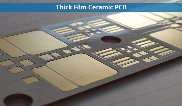
Thick Film Ceramic PCB
In Ceramic PCB manufacturing, especially the ceramic metallization, a thick film is a layer of copper deposited on the ceramic (Al2O3, AlN) substrates. The bonded copper thickness to the substrates ranges from 10μm (≈1/3oz) to 140μm (4oz) by DPC technology and traditional PCB plating technology, from 140μm (4oz) to 350μm (10oz) by DBC technology, and up to 800μm (22.8oz) by AMB technology.
Thick Film Ceramic PCB
Thick Film Deposition Technologies
The process of applying a thick layer to a substrate is thick-film deposition – any technique for depositing a thick copper onto a ceramic substrate or onto previously deposited layers. “Thick” is a relative term, but most film deposition techniques control layer thickness more than tens of microns (μm). There are 3 thick-film deposition technologies to realize thick copper film on ceramic substrates:
- Active Metal Brazing (AMB): Unlike DBC, Active Metal Brazing forms the substrates without metallization. Under a high temperature vacuum the copper is joined (brazed) direct to the ceramic base. This offers a high reliability substrate with unique heat dissipation. The brazing technology also enables copper weights of up to 800μm on thin ceramic substrates. These heavy copper materials make AMB ideal for power electronics.
- Direct Plated Copper (DPC): DPC is recent development in the field of Ceramic Substrate PCBs and was the breakthrough that made ceramics much more viable to designers. DPC involves vacuum sputtering under high temperature and pressure conditions to plate the copper to the substrate. The addition of a thin film titanium (Ti) layer acts as a bonding interface between the copper and ceramic layers. DPC can only deposit very thin copper film onto the ceramic substrate, need to combine traditional plating process to reach thick copper thickness requirement.
- Direct Bonded Copper (DBC): With DBC the copper is bonded to the Ceramic substrates on one or both sides using a high-temperature oxidation process. It offers options of heavy copper thickness -140μm (4oz)-350μm (10oz). The copper and substrate are heated in an atmosphere of nitrogen containing about 30ppm of oxygen; under these conditions, a copper-oxygen eutectic forms which bonds successfully both to copper and the oxides used as substrates. With DBC the copper layers can then be etched using standard PCB technology to form required circuit.
With different thick copper layer deposition technologies, we divide Ceramic PCBs into 3 types, including AMB Ceramic PCB, DPC Ceramic PCB and DBC Ceramic PCB. But in MADPCB, DBC is replaced by advanced DPC technology, and we only use DPC technology to fabricate thick and thin film ceramic PCBs now.
Ceramic PCB Manufacturing Capabilities
|
Property |
AMB | DPC |
DBC |
|
Compatible Substrates |
AlN / SiN | Al2O3 / AlN / SiN |
Al2O3 / AlN / SiN |
|
Substrate Thickness (mm) |
0.25/0.32/0.38/0.63 /1.0 |
0.25/0.38/0.5/0.635 1.0/1.5/2.0 |
0.25/0.38/0.5/0.635 |
|
Copper Weight |
See Below | 10 – 140 |
140 – 350 |
|
Panel Sizes |
Standard: 115 x 115 | Standard: 115 x 115 | Standard: 115 x 115 |
| Special: Up to 170 x 250 | Special: Up to 170 x 250 |
Special: Up to 170 x 250 |
|
|
Finish Options |
ENIG/ENEPIG/EPIG/Immersion Silver/Immersion Tin/OSP |
||
|
Min Trace Width |
Dependant on Cu Weight | 0.1 |
Dependant on Cu Weight |
|
Min Hole Diameter |
0.08 | 0.08 |
0.08 |
|
PTH |
N/A | 5:01 |
N/A |