What Is the Aspect Ratio in PCB?
Aspect Ratio (AR) is the ratio of the drilling depth compared to the drilling diameter of the smallest hole drilled in the same PCB. The drilling methods can be either CNC mechanical drilling, or laser drilling. The drilling depth is without copper plating, solder mask, surface finish or silkscreen. In PCB fabrication, the larger the ratio the more difficult it is to realize reliable plating.
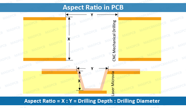
Aspect Ratio in PCB
As the ratio increases, more plating will be required, and thus there is a proportional increase in the risk of cracking due to expansion during the PCB assembly process. A lower ratio will have the benefit of stronger vias that provide better electrical connections. Keeping your PCB AR lower will ensure consistent plating throughout the via and will allow for greater strength throughout the life of the printed circuit board.
Capabilities of NC Drilling Vias
|
Min NC Drilling |
Available Aspect Ratio |
Max Available |
|
0.15mm |
<=8:1 |
1.2mm |
|
0.20mm |
<=10:1 |
2.0mm |
|
0.25mm |
<=12:1 |
3.0mm |
Capabilities of Laser Ablated Microvias
| Smallest Laser Microvia | 3mil (0.075mm) |
| Largest Laser Microvia | 10mil (0.25mm) |
| Microvia Aspect Ratio | Standard: 0.75:1 Advanced: 1:1 |
| Capture Pad Size | Standard: μVia +0.008 Advanced: μVia +0.006 |
| Land Pad Size | Standard: μVia + 8mil Advanced: μVia + 6mil |
| Stacked Microvia | Yes |
| Type I Capabilities | Yes |
| Type II Capabilities | Yes |
| Type III Capabilities | Design Dependent |
| Copper Filled Microvias | Yes |
According to the IPC-2221A and IPC-222 design guidelines a maximum AR 8:1 is recommended for through-hole vias. Likewise, a minimum drill diameter of 0.20mm is recommended for a 1.60mm standard PCB thickness. But at MADPCB, we can reach 10:1 and 12:1 for through-hole boards, and reach 0.75:1 and 1:1 for microvia HDI PCBs.
These parameters are absolutely suitable for PCB production and they are also recommended by MADPCB. For high IPC Class 3 reliability requirements like this are essential. Due to reliability reasons, it is not possible to arbitrarily decrease the via pad size and the hole diameter.