Plating on a PCB refers to the electrochemical process by which a metal is deposited onto the surface of the circuit board, and inside the plated through-holes.
PCB Plating
PCB plating may be defined as following:
- Via Plating: the process of filling a drilled hole with the material copper to provide a path for current from a surface of the board to an inner layer, between two inner layers or from one surface to the other. These plated through holes (PTHs) are better known as vias.
- Surface Plating or Finishing: the process of covering surface copper traces with Gold, Silver, Tin or Nickel to protect against the environment, oxidation, moisture, and contamination, and to provide a more suitable for soldering components during PCB assembly.
Both of the processes listed above may be referred to as PCB plating. And although the primary objective of both is to help facilitate good current flow along PCB paths, there are differences in the materials used.
As you probably suspect, your choice of PCB surface finish matters, as there are advantages and disadvantages to each type. Similarly, there are PCB plating process options and design selections should be based on their attributes.
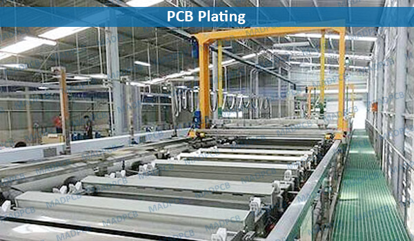
PCB Plating Process
The technicians load the PCB panels onto the flight bars. They check all the clamps to ensure a good electrical connection. The panels themselves act as cathodes for electroplating and we can plate the hole walls contributes to the conductive carbon layer already deposited there. They start the automated plating line. The copper surface of the panels is cleaned and activated in a number of baths and then electroplated. The whole process is computer controlled to ensure that each set or flight of panels stay in each bath exactly the right amount of time.
The baths are designed to produce an even copper thickness across the panel. Modern chemical solutions also have good “throwing power” to produce an even thickness of copper right through the hole.
The PCB plating process is an important step of the PCB fabrication process to ensure the best surface for PCB assembly is available and that your traces and vias are reliable and durable. At MADPCB’s smart manufacturing facility, we provide various options for the plating of your circuit boards that meet or exceed IPC 2 and 3 standards and your expected quality.