What is a Logic Gate?
A Logic Gate is an idealized model of computation or physical electronic device implementing a Boolean function, a logical operation performed on one or more binary inputs that produces a single binary output. Depending on the context, the term may refer to an ideal logic gate, one that has for instance zero rise time and unlimited fan-out, or it may refer to a non-ideal physical device.
Logic gates are primarily implemented using diodes or transistors acting as electronic switches, but can also be constructed using vacuum tubes, electromagnetic relays (relay logic), fluidic logic, pneumatic logic, optics, molecules, or even mechanical elements. With amplification, logic gates can be cascaded in the same way that Boolean functions can be composed, allowing the construction of a physical model of all Boolean logic, and therefore, all of the algorithms and mathematics that can be described with Boolean logic.
See Logic Circuits
Electronic Gates
A functionally complete logic system may be composed of relays, valves (vacuum tubes), or transistors. The simplest family of logic gates uses bipolar transistors, which is called resistor-transistor logic (RTL). Unlike simple diode logic gates (which do not have a gain element), RTL gates can be cascaded indefinitely to produce more complex logic functions. RTL gates were used in early integrated circuits (ICs). For higher speed and better density, the resistors used in RTL were replaced by diodes resulting in diode-transistor (DTL). Transistor-transistor logic (TTL) then supplanted DTL. As ICs became more complex, bipolar transistors were replaced with smaller MOSFETs. To reduce power consumption still further, most contemporary chip implementations of digital systems now use CMOS logic. CMOS uses complementary (both n-channel and p-channel) MOSFET devices to achieve a high speed with low power dissipation.
Electronic logic gates differ significantly from their relay-and-switch equivalents. They are much faster, consume much less power, and are much smaller (all by a factor of a million or more in most cases). Also, there is a fundamental structural difference. The switch circuit creates a continuous metallic path for current to flow (in either direction) between its input and its output. The semiconductor logic gates, on the other hand, acts as a high-gain voltage amplifier, which sinks a tiny current at its input and produces a low-impedance voltage at its output. It is not possible for current to flow between the output and the input of a semiconductor logic gate.
Another important advantage of standardized IC logic families, such as the 7400 and 4000 families, is that they can be cascaded. This means that the output of one gate can be wired to the inputs of one or several other gates, and so on. Systems with varying degrees of complexity can be built without great concern of the designer for the internal workings of the gates, provided the limitations of each integrated circuit are considered.
The output of one gate can only drive a finite number of inputs to other gates, a number called the ‘fan-out limit’. Also, there is always a delay, called the ‘propagation delay‘, from a change in input of a gate to the corresponding change in its output. When gates are cascaded, the total propagation delay is approximately the sum of the individual delays, an effect which can become a problem in high-speed circuits. Additional delay can be caused when many inputs are connected to an output, due to the distributed capacitance of all the inputs and wiring and the finite amount of current that each output can provide.
7 Basic Logic Gates
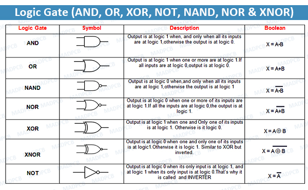
Logic Gate (AND, OR, XOR, NOT, NAND, NOR & XNOR)
- AND: the AND gate is so named because, if 0 is called “false” and 1 is called “true”, the gate acts in the same way as the logical “and” operator. The figure shows the circuit symbol and logic combinations for an AND gate. (In the symbol, the input terminals are at left and the output terminal is at right.) The output is “true” when both inputs are “true”. Otherwise, the output is “false”. In other words, the output is 1 only when both inputs one AND two are 1.
- OR: the OR gate gets its name from the fact that it behaves after the fashion of the logical inclusive “or.” The output is “true” if either or both of the inputs are “true.” If both inputs are “false,” then the output is “false.” In other words, for the output to be 1, at least input one OR two must be 1.
- XOR: the XOR (exclusive-OR) gate acts in the same way as the logical “either/or.” The output is “true” if either, but not both, of the inputs are “true.” The output is “false” if both inputs are “false” or if both inputs are “true.” Another way of looking at this circuit is to observe that the output is 1 if the inputs are different, but 0 if the inputs are the same.
- NOT gate: a logical inverter, sometimes called a NOT gate to differentiate it from other types of electronic inverter devices, has only one input. It reverses the logic state. If the input is 1, then the output is 0. If the input is 0, then the output is 1.
- NAND gate: the NAND gate operates as an AND gate followed by a NOT gate. It acts in the manner of the logical operation “and” followed by negation. The output is “false” if both inputs are “true.” Otherwise, the output is “true.”
- NOR gate: the NOR gate is a combination OR gate followed by an inverter. Its output is “true” if both inputs are “false.” Otherwise, the output is “false.”
- XNOR gate: the XNOR (exclusive-NOR) gate is a combination XOR gate followed by an inverter. Its output is “true” if the inputs are the same, and “false” if the inputs are different.
Complex operations can be performed using combinations of these logic gates. In theory, there is no limit to the number of gates that can be arrayed together in a single device. But in practice, there is a limit to the number of gates that can be packed into a given physical space. Arrays of logic gates are found in digital ICs. As IC technology advances, the required physical volume for each individual logic gate decreases and digital devices of the same or smaller size become capable of performing ever-more-complicated operations at ever-increasing speeds.
Composition of Logic Gates
High or low binary conditions are represented by different voltage levels. The logic state of a terminal can, and generally does, often change as the circuit processes data. In most logic gates, the low state is approximately zero volts (0 V), while the high state is approximately five volts positive (+5 V).
Logic gates can be made of resistors and transistors or diodes. A resistor can commonly be used as a pull-up or pull-down resistor. Pull-up and pull-down resistors are used when there are any unused logic gate inputs to connect to a logic level 1 or 0. This prevents any false switching of the gate. Pull-up resistors are connected to Vcc (+5V), and pull-down resistors are connected to ground (0 V).
Commonly used logic gates are TTL and CMOS. TTL, or Transistor-Transistor Logic, ICs will use NPN and PNP type Bipolar Junction Transistors. CMOS, or Complementary Metal-Oxide-Silicon, ICs are constructed from MOSFET or JFET type Field Effect Transistors. TTL IC’s may commonly be labeled as the 7400 series of chips, while CMOS ICs may often be marked as a 4000 series of chips.