What’s QFN Package?
Quad Flat No Leads Package (QFN) is a very small square-shaped or rectangular surface-mount plastic package with no leads. It is basically a Quad Flat Package (QFP), except for the absence of leads protruding from its sides.
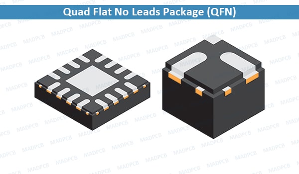
Quad Flat No Leads Package (QFN)
Metal pads or lands around the periphery of the bottom of the QFN package serve as electrical connection points to the outside world. Because the QFN has no leads and has shorter bond wire lengths, it exhibits less inductance than leaded packages and therefore provides a higher electrical performance. The QFN package also includes an exposed thermal pad at the package bottom to facilitate heat dissipation from the die.
| Properties of Some Examples | ||||
| Package Type | No. of Pads | Body Size | Body Thickness | Pad Pitch |
| QFN-16 | 16 | 3 x 3 mm | 0.9 mm | 0.5 mm |
| QFN-24 | 24 | 4 x 4 mm | 0.9 mm | 0.5 mm |
| QFN-32 | 32 | 5 x 5 mm | 0.9 mm | 0.5 mm |
| QFN-44 | 32 | 5 x 5 mm | 0.9 mm | 0.5 mm |
| QFN-50 | 50 | 5 x 10 mm | 1.0 mm | 0.5 mm |
| QFN-72 | 72 | 10 x 10 mm | 0.9 mm | 0.5 mm |
Different Types of QFNs
The surface-mount IC packages that are assembled on a circuit board are available in different types. The most popular ones among these are the QFN packages. These miniature packages are suitable for consumer, industrial, automotive, and power applications. When it comes to these packages, we have a lot to learn regarding their types, features, design, and assembly.
Based on the method of molding, the QFN packages are classified into Punch-Type and Sawn-Type packages.
- Punch-Type: In punch-type singulation, the package is molded in the single mold cavity format and is separated using a punch tool. This means that only a single package is molded into shape using this method.
- Sawn-Type: These packages are molded using the mold array process (MAP). This method involves cutting a large set of packages into parts. A final saw process helps to separate the sawn-type packages into individual packages.
QFN Assembly
The following are the basic steps involved in the surface-mount assembly of the QFN components:
- Solder-paste printing: Solder paste printing is the process of uniformly spreading the solder paste on the board before placement of components.
- Component placement: The QFN IC components are mounted on the printed circuit board as per the layout decided during the PCB design stage. Since these components have high interconnection density, precise and accurate pick and place tools are used.
- Pre-reflow inspection: Pre-reflow inspection is done to ensure that the board is ready to go into the reflow oven. This helps to remove contaminants on the surface of the board that may interfere with the soldering process.
- Reflow soldering: QFN components are commonly soldered using reflow soldering.
- Post reflow inspection: This inspection is done to check the quality of the soldering.
A proper PCB footprint and stencil design are required for the assembled components to operate as per the design intent.
How to Solder QFN on to a PCB?
Soldering is a part of the QFN assembly process. During the assembly process, the components are mounted after solder paste screening. After components are mounted using a pick and place tool, they are soldered using reflow soldering. When the PCB goes into a reflow oven, the temperature inside will make certain areas of the board heat faster than the rest. The heavier components and large copper areas will take more time to get heated.
The top surface temperature of the QFN package is monitored using thermocouples throughout the process. This is to check that the peak package body temperature (TP) does not exceed the standard values.
How are the QFN Solder Joints Inspected?
The solder joints of the QFN components are formed underneath the package. Hence for the inspection of these, optical inspection and X-ray inspection are used.
Rework on Assembled Components
If a defect is noticed post assembly on any QFN component, that particular component can be removed and replaced. Special rework stations are available for this purpose. A rework station should have the following components.
- Split-light system: acts as a vision system to observe the bottom side of the package and the site on the PCB.
- An X-Y table for alignment.
- A hot-air system with top and bottom heaters for component removal.
The procedure for rework is given below.
- A pre-bake process is done before heating to avoid any moisture-related failures of the board and the components.
- The next step is de-soldering and the temperature profile of the board and the components should be kept in mind.
- Once de-soldering is done, the component should be mechanically removed. For large components, pipettes can be used and for smaller ones, tweezers are a good option.
- After removal, the PCB pads should be cleaned to remove any solder residue. This also prepares the site for the new component placement.
- The placement of the new component takes place through the same steps mentioned earlier during PCB assembly.