What Is WLCSP?
WLCSP or WL-CSP (Wafer-level Chip Scale Packaging) (sometimes WCSP) refers to the technology of packaging an integrated circuit at the wafer level, instead of the traditional process of assembling individual units in packages after dicing them from a wafer. This process is an extension of the wafer fabrication process, where the device interconnects and protection is accomplished using the traditional fab processes and tools. In the final form, the device is a die with an array pattern of bumps or solder balls attached at an I/O pitch that is compatible with traditional printed circuit board (PCB) assembly processes. WLCSP is a true chip-scale packaging (CSP) technology, since the resulting package is of the same size. WLCSP technology differs from other ball-grid array (BGA) and laminate-based CSPs in that no bond wires or interposer connections are required. The key advantages of the WLCSP is the die to PCB inductance is minimized, reduced package size, and enhanced thermal conduction characteristics.
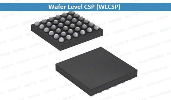
Wafer Level CSP (WLCSP)
WLCSP Assembly
In PCB design, proper PCB footprint and stencil designs are critical to ensure high surface mount assembly yields, and electrical and mechanical performance.
The WLCSP package is comparatively small in size. For better accuracy, it is recommended to use automated fine-pitch placement
machines with vision alignment instead of chip-shooters to place the parts. Local fiducials are required on the board to support the vision
systems.
Pick and Place systems using mechanical centering are not recommended due to the high potential for mechanical damage to the WLCSP
device. Ensure minimal pick-and-place force is used to avoid damage, with all vertical compression forces controlled and monitored.
Z-height control methods are recommended over force control. Freescale recommends the use of low-force nozzle options and compliant
tip materials to further avoid any physical damage to the WLCSP device. Use only vacuum pencil with compliant tip material whenever
manual handling is required.
All assemblers of WLCSP components are encouraged to conduct placement accuracy studies to provide factual local knowledge about
compensations needed for this package type. Freescale cannot anticipate the range of placement equipment and settings possible for
package placement and therefore cannot make a generic recommendation on how to compensate for WLCSP interchangeability.
Temperature profile is the most important control in reflow soldering and it must be fine-tuned to establish a robust process. The actual
profile depends on several factors, including complexity or products, oven type, solder type, temperature difference across the PCB, oven
and thermocouple tolerances, etc. All of Freescale’s WLCSP devices are qualified at Moisture Sensitivity Level 1 at 260°C. The maximum
temperature at the component body should not exceed this level. Actual reflow temperature settings need to be determined by the
end-user, based on thermal loading effects and on solder paste vendor recommendations.
The solder joints of WLCSP parts are formed underneath the package. To verify any open or short-circuits (bridging) after reflow,
non-destructive optical inspection and X-ray inspection are recommended to verify any open or short-circuit after reflow soldering.