What Is Micro BGA (Ball Grid Array), MicroBGA, or μBGA?
The Micro BGA is one of the most advanced surface mount devices (SMDs) and is quickly becoming the package of choice for the electronic circuit designer. A micro BGA is a subclass of the generic BGA. A typical BGA package has ball-to-ball spacing of 1.0mm or 0.8mm, whereas a typical micro BGA package has a pitch of about 0.4mm or less. This permits package size reduction, among other advantages, plus μBGAs can be placed in close proximity on a printed circuit board (PCB).
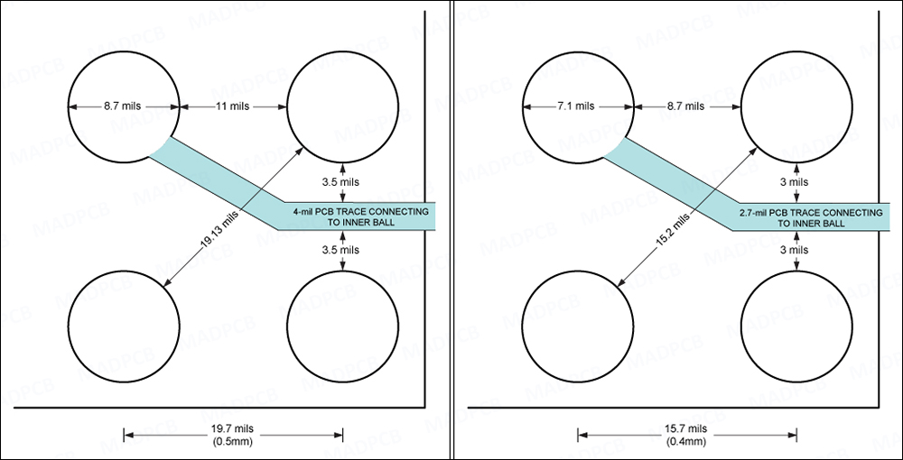
PCB Trace Routing for 0.5mm and 0.4mm Pitch IC
Packaging technology plays a key role in device performance. In the past few years, innovative technologies have reduced chip delay in the actual IC semiconductor material. However, in a packaged IC, signal delay has not been able to reduce as much. Thus, packages have become a bottleneck in high-speed systems. One of the best solutions is the micro BGA because it exhibits better chip delay performance when compared to other technologies.
Benefits of Micro BGA
Since the micro BGA package is more compact than other SMT devices, it has a shorter contact length from the device pin to the outside world. Therefore, it provides a lower inductance/impedance path to all signals. It can keep pace with the advancement of IC semiconductor and logic implementation technologies and has minimized the signal losses by increasing the packaging density and reducing the packaging delay.
A micro BGA’s electrical performance shows that it has low resistance, capacitance and inductance of the short beam leads. For high performance applications, an optional ground plane further reduces the self and mutual inductance, as well as cross talk.
While Micro BGAs represent a major innovation in component packaging, they pose a significant challenge for PCB design. A typical micro BGA package feature 0.4mm pitch, but the latest generation of fine pitch BGAs are as small as 0.3mm and 0.25mm pitch. PCB designers must first find easier ways for pin fanout/routing solutions for 0.4mm pitch BGAs, otherwise, routing complications can result. Consequently, those complications can cause an increase in layer count and sometimes call for high-end fabrication requirements.
This means that before finalizing a microBGA package for design, the designer should carefully analyze the micro-BGA device’s details and make sure the balls’ pin pitch allows for all traces fanout/routing without using unnecessary special manufacturing requirements, and that it can be done within the allowed number of layers.
The designer’s intent is to optimize the number of layers required to route high pin count packages without affecting their performance. The pin assignment and pin grounding of the mircoBGAs can also to be modified to enable efficient board routing with an optimum number of required board layers.
NSMD and SMD Pads of Micro BGA
Chip manufacturers have detailed datasheets that include recommended land patterns. There are normally two types of land patterns used for BGA pads: Non-Solder Mask-Defined (NSMD) pads and Solder Mask-Defined (SMD) pads.
NSMD pads have solder mask openings that is larger than the pads, whereas SMD pads have a solder mask opening that is smaller than the copper pad. Most vendors suggest the use of NSMD because it provides tighter control of copper artwork registration compared to the positional tolerance of the solder mask process. This becomes more important when the PCB designer deals with fine pitch components, like micro BGA package.
Micro BGA Fanout in PCB Design
The fanout/routing technique takes into account such factors as ball pitch, land diameter, number I/O pins, via type, pad size, trace width/spacing and the number of layers required to escape the micro BGA.
It’s not appropriate to have a traditional dog-bone fanout pattern for a microBGA because of its narrow pitch. This means either via-in-pad or blind/buried vias are used. The via-in-pad approach places a via directly under the device’s contact pads, filled with a conductive material, usually silver, which can provide a fairly flat surface. This allows higher component density and improved routing.
It’s obvious the traditional approach of BGA fan-out is not workable here. It means the designer has to use either via-in-pad or blind/buried vias or a combination of both. In order to make the design cost effective for PCB manufacturing, it’s better to avoid blind and buried vias, but it really depends on the micro BGA package size and its pins assignment.
Micro BGA package increases the level of design complexity. Its narrow pitch creates a challenge for the PCB layout, as does the greater number of pins connecting to the design in a smaller area compared to a conventional BGA. Similarly, board fabrication may be required to undergo advanced techniques, resulting in cost increases. Circuit board manufacturer need to develop easier PCB fabrication process for such components and should be prepared for further pitch components.
A micro BGA comes with considerable electrical and physical benefits. However, as with any technology, a μBGA is not without problems. For example, microBGA expertise is not commonly available, rework methods are more difficult, solder joint reliability is more critical, voiding becomes an increasingly critical issue and micro BGA assembly inspection is more difficult.