What Is DSBGA?
Die Size Ball Grid Array (DSBGA), also known as Wafer Level Chip Scale Package (WLCSP), refers to packaging an IC in wafer form, in contrast to packaging an IC after it has been singulated from the wafer. It uses a copper redistribution layer to connect the silicon interconnect to an array of solder balls. The package size is equal to the silicon die size, enabling WLCSP to have the smallest form factor compared to other package types. WlCSP is a great package solution for space-constrained applications such as mobile or wearables.
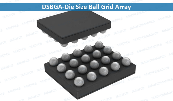
DSBGA-Die Size Ball Grid Array
DSBGA Technology
It is the broader term for WLCSP technologies with the following features:
- Package size equal to die size
- Smallest footprint per I/O count
- Interconnect layout available in 0.3mm, 0.35mm, 0.4mm, or 0.5mm pitch
- No interpose between the silicon IC and the printed circuit board
- The underfill should have a CTE closely matched to the CTE of the solder interconnect
- The underfill should have a Tg above the expected maximum exposure temperature
Typical DSBGA products have solder bumps located on the active side of silicon IC. The DSBGA manufacturing process steps include the following:
- Standard wafer fabrication process
- Wafer re-passivation
- Deposition of solder bumps on I/O pads
- Back-grinding
- Application of protective encapsulation coating
- Testing using wafer sort platform
- Laser marketing
- Singulation
- Packing in tape and reel
The package is assembled on PCB using standard surface mount assembly technique (SMT).
DSBGA Surface Mounting Assembly Considerations
The DSBGA package requires specific mounting technique, the SMT operations include:
- Printing solder paste onto a PCB
- Component placement using standard pick and place machine
- Reflow soldering and cleaning (depending on flux type)
Advantages of DSBGA during SMT assembly include:
- Standard SMT pick and place machine
- Standard reflow process
PCB Layout when Using DSBGA: NSMD vs. SMD
Two types of PCB land patterns are used for surface mount packages:
- Non-solder mask defined (NSMD)
- Solder mask defined (SMD)
- The NSMD configuration is preferred due to its tighter control of the copper etch process and a reduction in the stress concentration points on the PCB side compared to SMD configuration.
- A copper layer thickness of less than 1oz is recommended to achieve higher solder joint stand-off. A 1oz (30μm) or greater copper thickness causes a lower effective solder joint stand-off, which can compromise solder joint reliability.
- For the NSMD pad geometry, the trace width at the connection to the land should not exceed 2/3 of the pad diameter.