What’s Ethernet and Gigabit Ethernet?
- In computer networking, Ethernet is a family of wired computer networking technologies commonly used in local area networks (LAN), metropolitan area networks (MAN) and wide area networks (WAN). It was commercially introduced in 1980 and first standardized in 1983 as IEEE 802.3. Ethernet has since been refined to support higher bit rates, a greater number of nodes, and longer link distances, but retains much backward compatibility. Over time, Ethernet has largely replaced competing wired LAN technologies such as Token Ring, FDDI, and ARCENT.
- In computer networking, Gigabit Ethernet (GbE or 1 GigE) is the term applied to transmitting Ethernet frames at a rate of a gigabit per second. The most popular variant 1000BASE-T is defined by the IEEE 802.3ab standard. It came into use in 1999, and has replaced Fast Ethernet in wired local networks due to its considerable speed improvement over Fast Ethernet, as well as its use of cables and equipment that are widely available, economical, and similar to previous standards.
Ethernet Routing for Signal Performance
Ethernet PCB routing is a formidable challenge as its high-speed means increased susceptibility to interface if routed carelessly. The most common speed today are 100Mbps, 1,000Mbps, and 10Gbps. Even at the lowest rate, you’ll want to muster all your knowledge and tread carefully in design.
An ethernet design that was routed without abiding by any specific rules is an invitation for disaster on the prototype PCB. In some instances, the firmware engineer testing the design would have difficulty establishing a connection on the port. Less severe, but equally troubling issues is to have unstable connections or limited speed due to signal integrity (SI) problems.
Troubleshooting ethernet issues after the PCB manufacturing and assembly is not easy. It’s better to get the design right during the design stage to prevent costly post-production issues.
Top Considerations for Ethernet PCB Routing
A typical ethernet design consists of the PHY component and the magnetics. The port Physical Layer (PHY) is a component that interfaces link-layer signaling to the physical layer’ analog differential analog signal.
*NOTE: A PHY, an abbreviation for “physical layer“, is an electronic circuit, usually implemented as an integrated circuit, required to implement physical layer functions of the OSI model in a network interface controller.
The magnetics, a common term used in ethernet PCB design, helps to isolate the internal circuitry from transient and common mode noise from external LAN cable. The signal traces that run between the magnetics and the PHY are high-speed analog and extremely sensitive to interference.
But your attention shouldn’t purely be focused on the PHY and magnetics. Most PCB designs involve an MAC of a microcontroller that interfaces with the PHY. The interface involved clocked signals that run up to 50MHz in the RMI protocol or 125MHz for SMII. You’ll want to pay equal attention to the digital connection between the MAC and PHY.
Electromagnetic interference is a real concern in PCB design as it involves bridging analog and high-speed digital signals. Clocking signal that drives the PHY and common mode noise from the LAN cable can cause interference to the Ethernet signals. Thus, component placement and routing strategies have a significant impact on routing.
Ethernet PCB Routing Guidelines
When tasked to design electronics that transmit over the ethernet, you’ll want to abide by these guidelines:
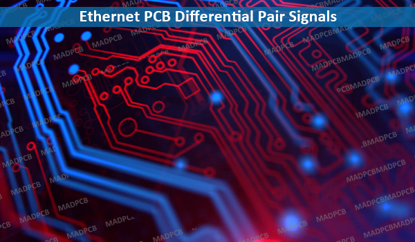
Ethernet PCB Differential Pair Signals
- Place crystal near to the PHY and keep the trace short.
- Keep the KHY at least 25mm away from the magnetics to prevent EMI issues. However, both the PHY and magnetics shouldn’t be too far apart as it attenuates the analog signal.
- Ensure that the differential pairs between the PHY and magnetics are routed in parallel and free from other high-speed signals.
- Pull up resistors on the PHY differential pair must be placed within 10mm from the traces.
- Place decoupling capacitors close to the power supply pins of PHY.
- Ensure a solid ground plane is present beneath the differential signals for the return paths. Never route signals never the split plane as that may cause EMI.
- No via should be present on the analog differential pairs to prevent impedance discontinuities. Keep them on the same plane.
- Avoid routing PHY differential pairs near the edge of the PCB to avoid interference coupling form external elements.
- Link layer signaling between PHY and MAC should be routed in parallel and maintain the same length.
Designing with ethernet components is a formidable challenge, but using the right PCB design software can minimize the risk of errors. The software helps enable system-level design and analysis, particularly useful in such PCB design applications.