What Is LVDA?
LVDS (Low-voltage Differential Signaling), also known as TIA/EIA-644, is a technical standard that specifies electrical characteristics of a differential, serial signaling standard, but it is not a protocol. LVDS operates at low power and can run at very high speeds using inexpensive twisted-pair copper cables. LVDS is a physical layer (PHY) specification only; many data communication standards and applications use it and add a data link layer as defined in the OSI model on top of it.
LVDS was introduced in 1994, and has become popular in products such as LCD-TVs, automotive infotainment systems, industrial cameras and machine vision, notebook and tablet computers, and communications systems. The typical applications are high-speed video, graphics, video camera data transfers, and general purpose computer buses.
Early on, the notebook computer and LCD display vendors commonly used the term LVDS instead of FPD-Link when referring to their protocol, and the term LVDS has mistakenly become synonymous with Flat Panel Display Link in the video-display engineering vocabulary.
PCB Design Guidelines for LVDS Technology
Technology advances has generated devices operating at clock speeds exceeding 100MHz. With higher clock rates and pico seconds edge rate devices, PCB interconnects act as transmission lines and should be treated as such. Reflections due to mismatched impedance, crosstalk, dielectric loss, skin effects, dispersion loss and reduction of noise margin are some of the undesirable events seen on high speed transmission lines. At the same time, the bandwidth limiting factors of the interconnect must be understood. It is these effects that greatly reduce the performance of Si once placed on a PCB.
Understanding controlled impedance, differential signaling layout, de-coupling, terminations, layer stack-up and stub effects, can minimize many pitfalls and reduce cycle time in designing PCB’s. This application note gives the PCB designer some common guidelines to follow in designing PCB’s for LVDS (Low Voltage Differential Signaling) technology.
Choosing the Proper Material for PCB
Proper selection of material for high-speed board is essential. As the signal propagates through the interconnect, due to the lossy nature of the interconnect, signal degradation occurs. Er (dielectric constant) of the material and loss tangent or tan delta (tanδ) are some of the key parameters that explain the lossy nature of PCB’s. Er relates to how much of the energy is lost in the material due to dissipation. Ideally, materials should be selected with the lowest Er and Tanδ. Table 1 below shows some typical numbers.
|
Material Selection |
Dielectric Constant (Er) |
Loss Tangent (Tanδ) |
| Air | 1.0 |
0 |
|
PTFE (Teflon) |
2.1-2.5 | 0.0002-0.002 |
| BT Resin | 2.9-3.9 |
0.003-0.012 |
|
Polyimide |
2.8-3.5 | 0.004-0.02 |
| Silica (Quartz) | 3.8-4.2 |
0.0006-0.005 |
|
Polyimide/Glass |
3.8-4.5 | 0.003-0.01 |
| Epoxy/Glass (FR-4) | 4.1-5.3 |
0.002-0.02 |
As the table above shows, Er is not a constant as we know it and can vary considerably. In most applications, FR-4 material is used, FR-4 material has acceptable performance up to the 100MHz range, beyond that Teflon should be considered. Teflon tends to be 4X more expensive than FR-4 but as Table 1 shows, Teflon has a lower Er thus low loss. The lower the Er, the faster the velocity of propagation (Equation), the faster the board. The key point to remember is to minimize signal degradation as much as possible.
Equation: √Er = C/V
Where:
C = 0.0118 in/ps (speed of light)
V = Velocity of Propagation
Er = dielectric constant
PCB manufacturers publish a datasheet along with their circuit boards. This article specifies the Er and Tanδ along with other electrical parameters. Due to process variation, both the Er and Tanδ can change from board to board. Ensure that your PCB manufacturer provides this data on the fabrication cation material of your circuit board.
You can think of fabricating a PCB board as laying a carpet. The fiberglass material is held together by epoxy material. Places where the weave is not tight is where the Er can change. Within a single FR-4 PCB a 10% variation of Er is not uncommon and this can alter the propagation velocity of the signal considerably. This can lead to skew issues on signal lines.
Microstrip or Stripline?
Microstrip is a PCB trace above the dielectric material whereas a stripline is embedded between the substrate. The decision to use either one mainly depends on the number of layer the boards will be constructed and the complexity of signal routing. Some designs use a combination of both. Usually, boards are either 4 layer or 6 and in some cases 8. Due to the high-speed nature of LVDS lines, they need to be separated from larger swing TTL lines to avoid crosstalk. This can be done by using signals on different layers in a PCB isolated by Power/GND planes.
Delay through a stripline is longer than that of microstrip. Typically, microstrip has a delay of 147 ps/in (FR-4) and stripline has a delay of 188 ps/in (FR-4). Striplines require more via’s than microstrip.
How to Calculate for Controlled Impedance (Single-Ended)?
For a microstrip transmission line,
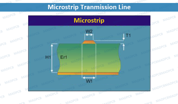
Microstrip Transmission Line
Microstrip Impedance
Where:
Z = trace impedance
Er = dielectric constant
Er = 4.5 (FR-4)
Er = 2.4 (Teflon)
w = width of trace
t = thickness of trace
h = prepreg (dielectric) height
Suggested typical numbers for LVDS PCB using microstrip are, t = 1.4mils, w = 12.0 mils and h = 8.1mils. This will give a 50ohm impedance from each trace to ground. The critical dimension that must also be taken into account is the distance between the signal pairs. This controls the differential impedance. It is recommended to hold this separation distance constant as much as possible (minor violations may occur at the device and connector connections). Next calculate the resulting differential impedance, and check that it matches the selected media (cable) differential mode characteristic impedance. If it is off substantially, the PCB trace dimensions should be adjusted to provide a match. To prevent reflections the PCB trace pair’s impedance should be matched to the interconnect/media. This is also the ideal value for the termination resistor that is connected across the pair at the receiver’s input. LDVS PCB manufacturing is also very important to reach impedance control tolerances.
For a stripline transmission line,
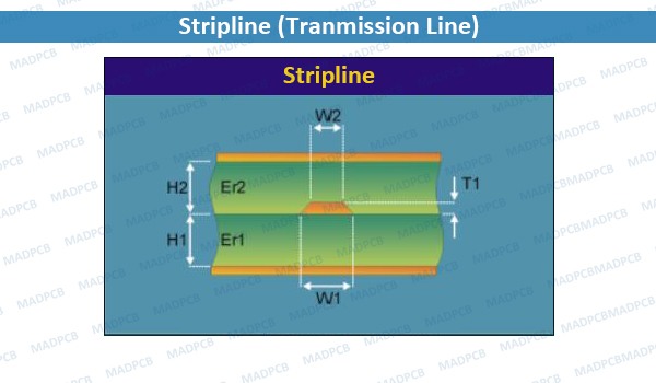
Stripline Microstrip Line
Stripline Impedance
Where:
Z = trace impedance
Er = dielectric constant
Er = 4.5 (FR-4)
Er = 2.4 (Teflon)
w = width of trace
t = thickness of trace
b = height between GND planes
h = prepreg (dielectric) height
Routing of Differential Lines
Differential lines have the characteristics of canceling common mode noise as it appears in phase on the two lines. This cancellation of common mode noise and magnetic effects allow differential drivers and receivers to operate over longer distances. But, this will only wok if the two traces are running close to each other. Care should be taken to keep the differential lines as parallel as possible. It is also critical to maintain the electrical/physical length of the two traces to be identical. This guarantees no skew on the line.
As sample layout of LVDS PCB traces shows the mitering effects done on the differential lines to match the electrical/physical lengths.
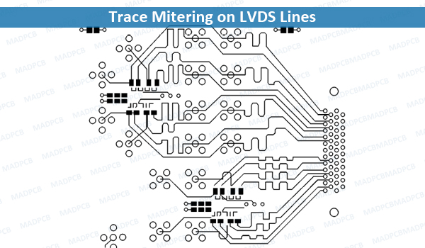
Trace Mitering on LVDS Lines
A sharp orthogonal turn (90°) should be avoided as it causes a sharp change in impedance. An arc should be used instead to round off the edge. This is critical in high frequency board layout.
Crosstalk between TTL and LVDS Lines
The PCB designer must note that all TTL/CMOS signal paths need to be isolated from the LVDS signal lines. Crosstalk is directly proportional to dv/dt. Since TTL/CMOS lines have a larger swing, crosstalk can easily occur if the TTL/CMOS paths are right next to the LVDS lines. Separation of the two technologies needs to be made either by increasing the distance between the two or running a ground trace between the two or isolating by using different planes.
When configuring a connector interface to a PCB and also for cable/connector interface from PCB to PCB, the designer should allow GND pins in between signal pairs on a connector as well as in a cable.
Mismatched Impedance
A PCB trace can be between 50ohm to 110ohm. As shown in figures below, this is dependent on the width and distance from the trace to ground. If a trace is wide and close to the ground plane, it is more capacitive and has an impedance close to 50ohm. If the trace is narrow and a good distance from a ground plane, it is more inductive and approaches 110ohm. Controlling the impedance to the desired value is very critical in avoiding reflections on the line.
Matching of impedance to reduce reflection should also be considered. Mismatch in impedance cuts into the noise margin and can ultimately render an application useless. The idea is to properly match the impedance of the media being driven with same value of termination resistor.
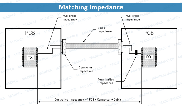
Matching Impedance
Termination Resistor Placement and Stubs
LVDS Drivers are current mode and they require the termination at the far end of the cable (PCB trace) and as close to the Receiver’s inputs as possible. An inch of PC trace stub can act as an unterminated transmission line causing reflection and this stub should be minimized. Multiple reflections cause ringing, overshoot and undershoot which reduces the noise margin.
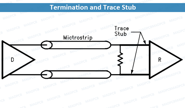
Termination and Trace Stub
In case of probing an LVDS transmission line, a high impedance (>1Mohm) scope probe should be used with a high bandwidth (BW) in the range of 3GHz-5GHz and low capacitance (0.25pF-0.5pF). Improper probing of a high speed transmission line can give deceiving results.
Choosing Termination Resistors (SMT)
Various vendors offer resistors in SMT form. A terminating resistor with radial shape can have too much inductance and this should be avoided. Only SMT type chip resistors with a tight tolerance should be used. Recommended tolerance is +/-1% of the termination value (100ohm typical). The user should always use Rt = Z0, termination resistor matched to the media. LVDS Drivers require a termination resistor with a range of 90ohm to 120ohm. SMT form factor also helps to reduce EMI.
Decoupling of VCC Line
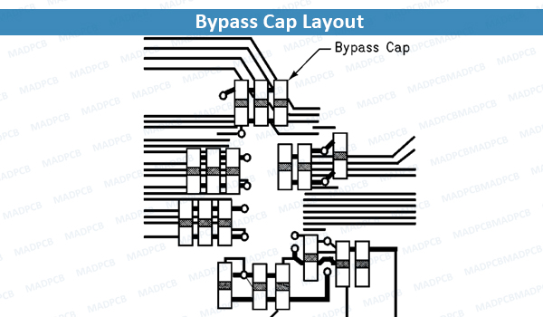
Both the main supply line and the device VCC pins should be properly decoupled. Bulk decoupling at the supply provides a constant low amplitude longer duration current and localized decoupling at the device provides high frequency energy required during SOS (simultaneous output switching) events. Proper decoupling reduces voltage spikes when all I/O pins are simultaneously switching. When decoupling the device VCC pins, the capacitors need to be placed as close to the device VCC pin as possible. Inductance caused by longer lead lengths must be avoided.
MLC (Multi-Layered Ceramic) capacitors in SMT form factor are recommended. Under high frequency, a capacitor is not an ideal element and can behave more like a LCR element. The L land and the R are parasitic effects that cause more problems. Since the goal is to reduce inductance in the line, short leads or SMT form factor is critical. It has been seen that a 2:1 length-width aspect ratio can have a 2nH of inductance but a 1:2 (width exceeds length) aspect ratio can cut down the inductance to 0.5nH in MLC capacitors. Fir the FPD Link chip set, the recommended bypassing is as follows:
Power Supply: 10.0μF tantalum electrolytic capacitor
VCC: 0.1μF, 0.01μF and 0.001μF
LVDS VCC: 0.1μF, 0.01μF and 0.001μF
PLL VCC: 0.1μF, 0.01μF and 0.001μF
A sample layout of FPD Link with multiple decoupling per VCC pin is illustrated below. VCC and GND trace width should be wider to reduce inductance and multiple via’s are also recommended to help reduce inductance.
In addition to low series inductance, lower effective series resistance (ESR) should be considered when choosing capacitors.
Bypass Cap Layout
Summary
High frequency effects should be minimized as much as possible when designing a PCB. Effects such as crosstalk, mismatched impedance, dielectric loss, skin effects, stubs can cut into the noise margin of the design. By following the PCB design guides mentioned in this application note, a designer can ensure success in developing a PCB for LVDS technology by avoiding all the high speed pit falls that are present in PCB designs today.