Table of Contents
Annular Ring
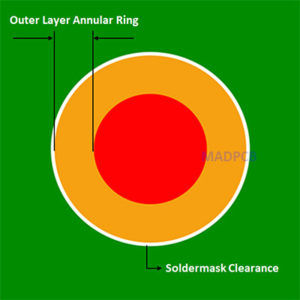
When need to connect traces to another layer in a multilayer board, or connect a part on the topside to an inner layer, a regular via needs extra room for a larger hole. You typically have to place a copper pad on your printed circuit board and drill a via on it to make the connection. The outer ring surrounding the via after drilling process constitutes the annular ring.
What’s Annular Ring (AR)?
An annular ring (AR) in PCB industry is the area of copper pad around a drilled and finished hole. The finished hole is a copper plated via, which can be a mechanically drilled plated hole (PTH) or a laser drilled microvia. All around the via there should be enough copper to form a solid connection between the copper traces and the via in a multi-layer PCB board. The main purpose of an AR ring is to establish a good connection between a via and the copper trace.
Soldermask Dam
PCB surface space is taken up by the hole’s annular ring, plus the minimum distance from pad to via for the solder mask web. The solder mask provides a dam that blocks the solder from flowing from the surface mount pad and down into the via during soldering. In addition to gravity, the surface tension of liquid solder causes the solder to be sucked into the hole during soldering.
Outer Annular Ring (OAR)
OAR Calculation:
- Outer Layer Annular Ring (OAR) = (Outer Layer Pad Diameter – Plated Hole Diameter)/2,
- OAR = (Copper Pad Diameter – Tool Size)/2,
- Tool Size = End Size + 0.10mm for all PTHs, +0.00mm for all NPTHs.
- Calculation for IAR on a copper pad of 0.60mm and finished hole size diameter of 0.30mm (PTH):
- IAR=[0.60mm–(0.30mm+0.10mm)]/2=0.10mm
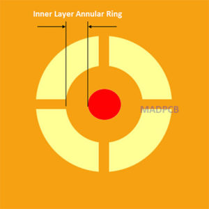
Inner Layer Annular Ring (IAR)
IAR Calculation:
- Inner Layer Annular Ring (IAR) = (Inner Layer Pad Diameter – Plated Hole Diameter)/2,
- IAR = (Copper Pad Diameter – Tool Size)/2,
- Tool Size = End Size + 0.10mm for all PTHs, +0.00mm for all NPTHs.
- Calculation for IAR on a copper pad of 0.50mm and finished hole size diameter of 0.20mm (PTH):
- IAR=[0.50mm–(0.20mm+0.10mm)]/2=0.10mm
Finished Annular Ring (FAR)
The area lying between the outer rim of the solder pad and the solder hole. As a result of the hole being drilling more or less off-center, the annular ring may be broken. This depends on the nominal outer diameter of the solder pad against the nominal diameter of the hole.
Minimum Annular Ring
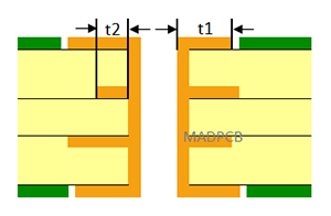
The minimum AR on printed circuit boards (PCBs) refers to the minimum amount of copper between the edge of the land (pad) and the edge of the plated via, which also referred to a supported hole. Sometimes, the traces on a circuit board are required to be connected to another layer. In such cases, the traces end up to on a pad. The via on the pad helps the trace to move from that pad and connect the other layer.
t1: the minimum annular ring on outer layers, must be >=0.05mm on the finished board.
t2: the minimum annular ring on inner layers, must be >=0.01mm on the finished board.
Reason for Using Annular Rings on PCB
The figure shows the relationship between hole and pad.
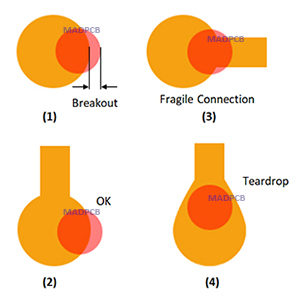
When using the smallest possible drill and pad, there is a chance that one or more holes will slightly overlap the edge of its pad [Figure 1]. Breakout is rare, but when PCB designers push the limits, this can happen to the smallest drills and pads.
The problem occurs when the breakout is in the same direction as a trace entering the pad [Figure 2]. When the hole overlaps the trace, there is a chance of an open circuit or a fragile connection [Figure 3] that could crack later. This decreases PCB yield, increases cost, and lowers reliability. This problem can be helped by using teardrops [Figure 4]. This pad shape extends the size of the pad but only in the direction of the trace. This acts as a larger pad but does not use any additional layout space. A teardrop pad can help push the process limits for the smallest possible annular ring without increasing cost.
Some PCB design tools don’t have the capability to add teardrops. In this case, the PCB manufacturer might be able to add them to your design. The result is a BGA layout with dog-bone shapes. The amount of copper added to make a teardrop dog-bone is small. Teardrops are often barely visible to the naked eye.
What do we allow in case of mis-alignment when drilling? Around PTH and NPTH, 90o is breakout allowed. And 90o breakout acceptable at land to trace junction (when trace not reduced by more than 20%).


