Table of Contents
What Is Copper Surface Roughness?
In high-speed design (HSD) and fabrication, we always meet the roughness of the conductor’ surface, which is called conductor or copper surface roughness. What’s copper surface roughness? As a PCB design and manufacturing company, MADPCB understands it well.
To the naked eye, coppers appear smooth, but at the microscopic level, copper foils and copper on laminates exhibit surface irregularities. This is surface roughness, and which has effects on the performance of high-speed PCBs.
Copper Foil Roughness Measurements
Surface roughness can be measured by mechanic and optical methods. Many sources report the Rz (peak to valley) profile as measured by a mechanical profilometer. However, in our experience, the Sq (RMS) profile as measured by white light interferometry of the treated side of copper foil correlates between conductor losses. Roughness data of electrodeposited (ED) and rolled (RA) copper foils with different thicknesses was obtained by using an optical surface profile. The surface roughness of different copper weights (oz) is different. Of course, the rolled copper with no surface treatment is typically the smoothest.
Electric Performance of Laminates
It has been well-known since the earliest days of microwave engineering with wave guides that the conductor surface roughness can substantially affect the conductor loss. In 1949, S.P. Morgan published results of numeric simulations that indicated that a factor of two increase in conductor loss could be caused by surface roughness. Hammerstad and Jensen, incorporated Morgan’s model, along with correlated data in microstrip design method. The H&J model became the “textbook” method for calculating the effect of surface roughness on conductor loss. More recently, at higher frequencies and with thinner laminates, it was found that H&J significantly under predicated the increase in conductor loss with surface roughness. The “Hall-Huray” model, developed from a “first principles” analysis, has been recently incorporated into commercial design software.
With modest adjustments to the input parameters, the Hall Hurray model can accurately predict conductor loss over a wide range of laminate thicknesses and frequencies.
Some studies have shown that the copper profile can affect the propagation constant, with higher profile foils leading to an apparent increase in the effective dielectric constant.
Mechanical Performance of Laminates
- Thermal Shock Resistance: Under some extreme conditions of rapid thermally cycling, electrodeposited (ED) copper may exhibit thermal stress cracks in narrow conductors. Under similar conditions, rolled copper has significantly improved resistance to cracking. Although electrodeposited copper has greater tensile strength and elongation before breaking, rolled copper has better elastic elongation before reaching permanent deformation.
- Foil Adhesion: Because of adhesion of resin systems to metals is predominantly mechanical, bond strength is directly related to the surface roughness of the treated foil side. Typically peel strength after thermal shock for 1oz copper foils.
- Bondability of Stripline Assemblies: For rolled copper-clad circuit boards, the surface roughness of the dielectric will give a poor mechanical bond, and surface treatment is necessary for reliable chemically boned assembly.
Skin Effect
The surface roughness of the conductor thereby causes the electromagnetic waves taking a path with a longer mean resulting in the increase in losses. Effectively, higher the degree of copper surface roughness, higher is the resistance from skin effects. When an electromagnetic wave propagates in a conductor, skin effect tends to change the electromagnetic wave’s current distribution to accumulate more towards the conductor’s surface rather than remaining deep inside the conductive copper.
Effects of Copper Surface Roughness
On high-speed PCBs, the effect of copper surface roughness on dielectric is negligible at frequencies below 1GHz. However, the frequency increases, the skin effect drives the current into the surface of the copper, dramatically increasing loss. When the copper surface is rough, the effective conductor length extends as current follows along the contours of the surface. The total loss comprises of the sum of the conductor loss and dielectric loss.
Whilst it may be possible to fabricate copper foil with a perfect smooth treatment, the foil-to-resin adhesion would be compromised. This would considerably increase the possibility of delamination during the thermal stress of the circuit board fabrication and assembly processes. For this reason, a reduced oxide coating is applied to the inner core layers to promote adhesion of the PP resin as it flows under the applied heat and pressure to cure.
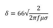
Skin effect is the tendency of an alternating current to become distributed within a conductor such that the current density is largest near the surface, and decreases with greater depths in the conductor. The higher the frequency, the greater the tendency for current to take the path of lower inductance on the outer surface of the conductor. The skin depth is given by:
Skin Depth Equation
Where:
δ = skin depth (in microns)
f = frequency (in MHz)
μ = magnetic permeability (4πx10-7H/m)
σ = copper conductivity (typically 5.6×10⁷S/m)
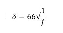
The skin depth (μm) can be approximated by:
Simplified Skin Depth Equation
Looking at this equation, it is apparent that skin depth decreases with increased frequency. At low frequency (1MHz), the skin depth is 66μm but this decreases to 0.66μm at 10GHz. So, at 10GHz, only the very outer surfaces of the copper trace carry the current. Also, the red horizontal lines represent the trace copper weight and thickness. This shows that at about 10MHz, a signal traveling in a 1/2oz (17.78μm) copper trace would not use the entire trace cross-section, but rather the skin effect would be dominant.
Most laminates are copper clad with either Rolled Annealed (RA) copper, electrodeposited (ED) copper or reverse-treated foil (RTF). RA copper is both smooth and consistent in thickness, but is the most expensive foil. ED copper has the roughest surface and depending on the application and speed requirements, may be perfectly adequate. RTF copper is smoother, and is much the same cost as ED. However, it does exhibit poor peel strength and is prone to delamination. So, it is a trade-off between performance and price.
RTF copper foils involve the subsequent treatment of the smooth side of the electrodeposited copper. Treatment layers are thin, rough coatings that improve adhesion of the base foil to the dielectric material.
To the naked eye, copper clad laminate appears smooth but at the microscopic level, all materials exhibit surface irregularities. If the average incline of the “teeth” of the conducting surface is 60°, forming an equilateral triangle, then the increase in surface resistance would be approximately twice that of a dead flat surface. Less severe geometries induce smaller effects. However, a better measure of the surface roughness is the root-mean-square (RMS) height (hRMS) of the surface bumps, since the exact profile cannot be established for a working design. Taking the worst case, equilateral ridge geometry as a guide, one would expect the RMS roughness to be in the order of 0.29mm times the average peak to valley roughness.
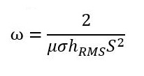
The onset frequency (ω) of the RMS surface roughness effect is given by:
Surface Roughness Effect Equation
where:
ω = onset frequency
μ = magnetic permeability (4πx10-7H/m)
σ = copper conductivity (5.98×10⁷S/m)
hRMS = root-mean-square Height for ED copper
Therefore, inserting the numbers into the above equation, the onset frequency of the RMS surface roughness effect is 1.28GHz for ED copper. The smoother the copper surface, the higher the frequency at which surface roughness takes effect.
Also, the effective dielectric constant and hence capacitance is increased due to the increased surface area of the teeth of the rough conductor. This, int turn, lowers the characteristic impedance slightly. The capacitance increases by about 5% for microstrip and 10% for stripline traces that exhibit more roughness. So the effect on impedance is -2% to -5%, respectively.
Surface Roughness in PCB Laminates
Although the surface roughness is not generally stated in material manufacturer’s datasheets, typical values are 3μm for the outer surface and 6μm for the inner surface. For example, Panasonic’s high-performance laminate, Megtron 6 (M6) core material, has a dielectric constant (Dk) of 3.4 and loss tangent (Df) of 0.004 at 18GHz. This material is available in standard ED, VLP, SVLP and HVLP (very/supper/hyper low profile) copper foil with average surface roughness of 7-8, 3-4 and 1.5-2μm respectively.
So, the smoothest surface HVLP material with 1.5μm average surface roughness, will therefore not exhibit any noticeable surface roughness effect up to 20GHz. Consequently, one would be well advised to take not of the surface roughness properties if your high speed design running over 1GHz to ensure you choose an appropriate material for the application.