Breakout in PCB means poor registration between the hole and the pad on a printed circuit board to the degree that the hole is not within the area of the pad.
Through hole pads need a solid annular ring for solderability. The annular ring is the metal between the outer perimeter of the pad and the hole wall. An annular ring’s size specification needs to be large enough to compensate for the drill to wander from the center of the hole. When the pad is too small, it might lead to a breakout, resulting in broken, incomplete circuits or improper soldering.
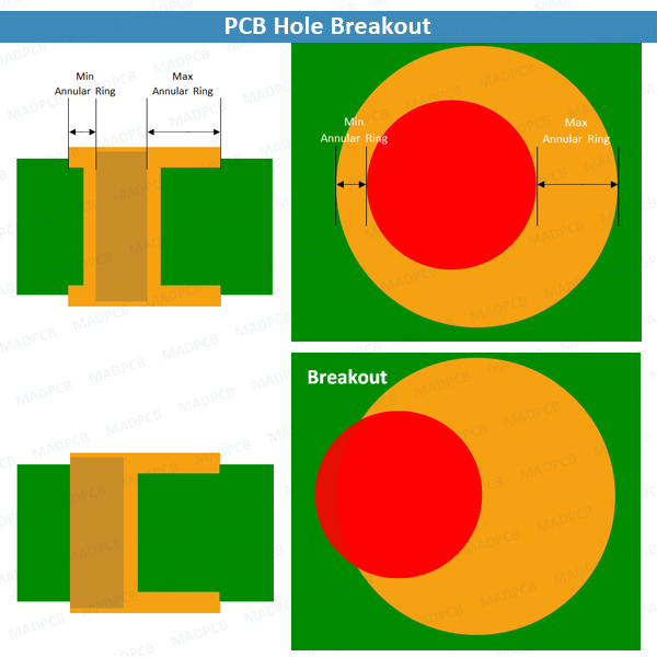
Annular Ring and Drill Holes
Annular rings are one of the biggest concerns of PCB designers. You know that you may place your via or PTH right in the middle of the pad in the design files, but it just does not mean that you will 100% avoid tangencies, or even worse, breakouts.
PCB Hole Breakout
The widths of the ring should be sufficiently thick to allow reliable electrical connection with via. The minimum length of the annular ring should be greater that or equal to the specified width for the design. An annular ring dimension that is less than the specified can interfere with the attachment of the component and a pad breakout (zero annular ring) condition associated with the area where the circuit enters the pad can reduce the current-carrying capacity of the circuit.
The drill hole must be drilled at the absolute center of the pad to form the annular ring or the minimum width of the annular ring must be above the specified value. Mis-registration of the via with respect to the land can lead to marginal interconnection that exhibit increased resistance and perhaps lead to reliability problems.
Breakout Probability
The smallest clearance 1mil, included to verify that the proper hole size was drilled, is intentionally designed to fail. The probability of breakout decreases from 98% for the 2mils designed clearance to zero for the 6 and 7mil clearances. If the breakout is not allowed, then designs fabricated by the PCB fabricator in this example would require annular rings of 6mil or larger for the microvias. By designing 5mil annular rings, the data estimate that 5% of the microvias will exhibit breakout.
During the PCB drilling process, there is possibility of misalignment of the drill bit which removes too much copper from the junctions of a via pad and PCB traces causing the possibility for a broken trace connection or too thin of a connection. In such cases, a teardrop can increase the tolerance of drill in the pad which can help reduce the rejection count in the PCB production.