What Is A Conductor in PCB?
PCB Conductor, Trace or Track, is a copper or constantan area on a PCB surface or internal layer, usually composed of lands (to which component leads are connected) and paths (traces).
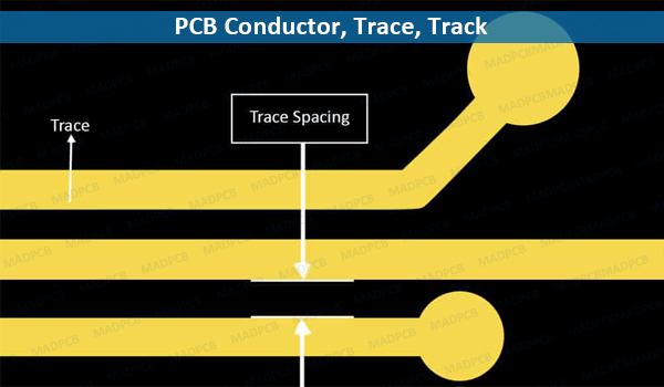
PCB Conductor, Trace, Track
The following table shows the maximum allowed conductor trace width with the minimum conductor trace spacing, depending on the respective copper thickness.
Conductor Width in Inner Layers
| Copper thickness | min. conductor trace width / space | min. annular ring |
| 12µm | 75µm/100µm** | 90µm |
| 18µm | 90µm | 90µm |
| 35µm | 100µm | 100µm |
| 70µm | 150µm | 150µm |
| 105µm | 250µm | 250µm |
| 140µm | 300µm | 300µm |
| 210µm | 500µm | 500µm |
Conductor Width in Outer Layers
| Final copper* | min. conductor trace width / space | min. annular ring |
| 30µm | 75µm/100µm** 90µm |
90µm 90µm |
| 35µm | 100µm | 100µm |
| 70µm | 150µm | 150µm |
| 105µm | 250µm | 250µm |
| 140µm | 300µm | 300µm |
| 210µm | 500µm | 500µm |
| 400µm | 900µm** | 900µm |
* After electroplating / ** prior data check necessary
Current Carrying Capacity of Conductors according to IPC-2221
Maximum current [A] subject to the temperature increase in degrees [°]
2 Layers – 35µm copper
| Trace Width | 10° | 20° | 30° | 40° | 50° | 60° | |
| 0.1mm | 4mil | 0.4A | 0.6A | 0.8A | 0.9A | 1.0A | 1.1A |
| 0.2mm | 8mil | 0.7A | 1.0A | 1.2A | 1.4A | 1.6A | 1.7A |
| 0.3mm | 12mil | 0.9A | 1.3A | 1.6A | 1.8A | 2.0A | 2.2A |
| 0.4mm | 16mil | 1.1A | 1.5A | 1.9A | 2.2A | 2.4A | 2.7A |
| 0.5mm | 20mil | 1.3A | 1.8A | 2.2A | 2.5A | 2.8A | 3.1A |
| 0.6mm | 24mil | 1.4A | 2.0A | 2.4A | 2.8A | 3.1A | 3.4A |
| 0.7mm | 28mil | 1.6A | 2.2A | 2.7A | 3.1A | 3.5A | 3.8A |
| 0.8mm | 32mil | 1.7A | 2.4A | 2.9A | 3.4A | 3.8A | 4.1A |
| 0.9mm | 36mil | 1.8A | 2.6A | 3.2A | 3.7A | 4.1A | 4.5A |
| 1.0mm | 40mil | 2.0A | 2.8A | 3.4A | 3.9A | 4.4A | 4.8A |
| 1.5mm | 60mil | 2.5A | 3.6A | 4.4A | 5.1A | 5.7A | 6.2A |
| 2.0mm | 80mil | 3.0A | 4.3A | 5.3A | 6.1A | 6.8A | 7.5A |
| 3.0mm | 120mil | 3.9A | 5.6A | 6.8A | 7.9A | 8.8A | 9.7A |
| 4.0mm | 160mil | 4.7A | 6.7A | 8.2A | 9.5A | 10.6A | 11.6A |
| 5.0mm | 200mil | 5.5A | 7.7A | 9.5A | 10.9A | 12.2A | 13.4A |
| 6.0mm | 240mil | 6.1A | 8.7A | 10.6A | 12.3A | 13.7A | 15.1A |
| 7.0mm | 280mil | 6.8A | 9.6A | 11.7A | 13.6A | 15.2A | 16.6A |
| 8.0mm | 320mil | 7.4A | 10.4A | 12.8A | 14.8A | 16.5A | 18.1A |
| 9.0mm | 360mil | 8.0A | 11.3A | 13.8A | 15.9A | 17.8A | 19.5A |
| 10.0mm | 400mil | 8.5A | 12.1A | 14.8A | 17.0A | 19.1A | 20.9A |
The calculation of the values is an approximation from the derived formulas of the IPC-2221 (see below). Deviation from DIN IEC 326 is due to the complexity of the topic. A rough estimate should always be possible.
The design guideline IPC-2221 (predecessor document: MILSTD 275) is the default data source for the DC temperature resistance of conductors. The measurements thereto come from the National Bureau of Standards (NBS) from the 1950s and refer to a 1.6mm thick PCB with a straight current-carrying conductor (thickness 35µm) and a 35µm Cu solid area on the back. They do not consider the surrounding medium (air pressure, motion), or the layout density.
In the 1960s the American magazine Design News published amended recommendations. In the mid-80s, in Germany the DIN IEC 326 comes out, which attends to this topic – the values obtained are quite similar to those from the Design News (with all advantages and disadvantages).
The tables specified here can therefore only be used to roughly estimate the temperature development.