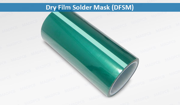
Dry Film Solder Mask (DFSM) is a water-based or solvent-based permanent material, which is packaged in rolls, the thicknesses are always 75μm and 100μm.
Dry Film Solder Mask (DFSM)
Application:
- Protection against oxidation of printed circuit board
- Prevents solder bridges forming between closely spaced solder pads
- Provides electrical insulation allowing higher voltage traces to be placed closer to one another.
It mainly used for circuit protection on the outer layer of flexible, rigid-flex printed circuit boards, IC substrates and other rigid boards. Dry film solder mask graphics has high resolution, suitable for high density and fine-line circuit boards. When developing with LDI technology, the registration will be much higher. Since it’s dry, it does not flow into through holes in boards to cause unqualified copper plating. It prevents solder mask bridges from solder connecting together while soldering in wave and reflow ovens. It protects the traces from mechanical damage or chemical corrosion. Besides, dry film solder mask is more expensive than liquid photoimageable (LPI) solder mask.
Dry Film Solder Mask General Processing Steps
- PCB surface preparation: ensuring the optimum adhesion of dry film mask and the surface to be laminated should be free
from dust particles, grease, oxides and other forms of surface contamination. - Hot Roll Lamination: using laminator machine to laminate the dry film mask to the board surface under heat and pressure. The laminator adjust the pressure to result in good vertical distribution of the mask, with no air inclusion between the traces.
- Exposure: non-UV and UV exposure are ok for different dry film masks. Cool down to the room ambient temperature after lamination before exposure. The amount of exposure energy the film receives will impact, resolution and adhesion, it can also impact the level of ionic contamination on the the film after develop or cure. Prior to developing a hold time of 15 to 30 minutes is recommended. Panels should be developed within 2 hours of exposure, but may be held for up to 75 hours prior to developing.
- Development: Unexposed DFSM can be easily developed using a mild alkaline solution in a totally aqueous, conveyorized spray developing unit. Development is followed by a thorough mains water rinsing, DI water rinsing and finally a turbine dry.
- Final Cure: Optimal physical, chemical, electrical environmental and end user assembly soldering performance properties of DFSM are obtained only after the final cure process. The final cure (cross linking process) is a two step process involving both high intensity UV. This is followed by a thermal cure.