Etch Back or Etchback, is the controlled removal by a chemical and plasma process, to a specific depth of nonmetallic materials from the sidewalls of holes in order to remove resin smear and to expose additional internal conductor surfaces.
Through Hole Etch Back in PCB
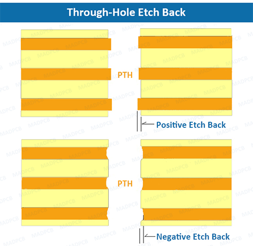
Through-hole etch back is a requirement that is sometimes specified in multilayer flexible circuits and combination multilayer rigid-flex boards. It specifically relates to the copper plated through-holes and the relative dimensions between the dielectric layers and copper layers.
- Micro Etch Process: To improve plating adhesion, the substrate or base laminate is often submerged or sprayed to remove a slight amount of copper in a micro-etch process. After the various circuit layers are laminated together the through-holes are drilled. This is then followed by a plasma etch step to remove organic resins such as smeared adhesives and dielectric debris. This sequence of processing insures the copper surface in the hole is free from contaminants. This is often referred to as desmearing.
- Plasma Etch Process: The plasma etch process is controlled to remove a specified amount of dielectric. Etching or removing the dielectric to expose the copper layers is called etchback or Positive Etchback. Etchback exposes more of the copper so a larger area can be plated. Essentially three sides of the copper layer can now be plated. This physical feature is used to create a more reliable plated through-hole. Negative Etchback is when the copper layer is etched back from the through-hole barrel.
- IPC-6013 states that etchback shall expose at least 0.003 mm (0.001”) and a maximum of 0.08 mm (0.003”) of copper, when etchback is specified on the procurement documentation.
- IPC-6013 specifies a minimum negative etchback for Class 1, 2 and 3 circuits. Class 1: 25 µm (0.001”), Class 2: 25 µm (0.001”) and Class 3: 13 µm(0.0005”).