Etch Factor is the ratios of etch depth to the amount the resist is undercut during etching.
In PCB fabrication process, copper has to be removed from solid copper sheets for realizing conductive traces. The most commonly way to remove the copper is through a process called Etching. In PCB etching process, the copper traces and other features that are to be kept are covered in a resist that protects the copper from the chemical etching solution. The solution removes the exposed copper and the resist is also removed, then the height of the copper trace have material etched from them. This is called Undercut.
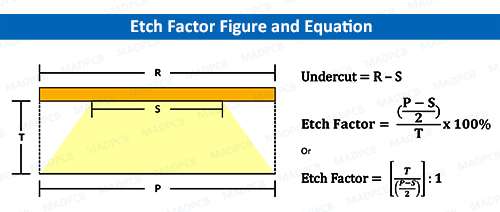
Etch Factor
From this figure, Undercut is the difference between the width of the developed resist line (R) and the final width of the etched feature across the top (S). The etch factor is the ratio between the difference in the widths of the widest and narrowest parts of the feature after etching is completed and the thickness of the copper etched. This can be expressed as a percentage as shown in the first equation or as a ratio as shown in the second. If it is 3:1 (1unit of sideways etch for every three units of downward etch) can also be expressed as a factor of 33% (the sideway etch is 33% of the downwards etch). The etching factor can also be thought of as an indication of how straight the sidewall of the feature is after the etching has been completed.
There are several things that need to be taken in consideration when using these definitions.
- Most importantly, undercut and etching factor are different entities, although we tend to use them interchangeably which can cause some confusion.
- Neither definition says anything about the relation of the widest part of the feature after etching is completed (P) to the width of the resist (R).
- Giving a number for undercut or etch factor without an indication of the relation of P to R after etching can be confusing or misleading.