What Is FET Biasing?
In electronics, Biasing is the setting of initial operating conditions (current and voltage) of an active device in an amplifier. Many electronic devices, such as diodes, transistors and vacuum tubes, whose function is processing time-varying (AC) signals, also require a steady (DC) current or voltage at their terminals to operate correctly. This current or voltage is a bias. The AC signal applied to them is super-positioned on this DC bias current or voltage.
For proper working of a transistor, it is essential to apply external voltages of correct polarity across its emitter-base and collector-base junctions. This is transistor biasing.
Unlike BJTs, thermal runaway does not occur with FETs. However, the wide differences in maximum and minimum transfer characteristics make ID levels unpredictable with simple fixed-gate bias voltage. To obtain reasonable limits on quiescent drain currents ID and drain-source voltage VDS, source resistor and potential divider bias techniques must be used. With few exceptions, MOSFET bias circuits are similar to those used for JFETs. Various FET biasing circuits in printed circuit board (PCB) design, fabrication and assembly are discussed below.
Fixed Bia
DC bias of a FET device needs setting of gate-source voltage VGS to give desired drain current ID. For a JFET drain current is limited by the saturation current IDS. Since the FET has such a high input impedance that no gate current flows and the DC voltage of the gate set by a voltage divider or a fixed battery voltage is not affected or loaded by the FET.
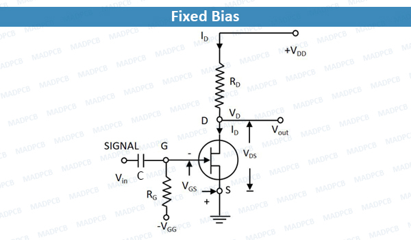
Fixed Bias Circuit
Fixed DC bias is obtained using a battery VQS. This battery ensures that the gate is always negative with respect to source and no current flows through resistor RG and gate terminal that is IG=0. The battery provides a voltage VGS to bias the N-channel JFET, but no resulting current is drawn from the battery VFF. Resistor RG is included to allow any AC signal applied through capacitor C to develop across RG. While an AC signal will develop across RG, the DC voltage drop across RG is equal to IGRG i.e. 0 volt.
The gate-source voltage VGS is then
VGS = -VG – Vg = -VGG – 0 = -VGG
The drain-source current ID is then fixed by the gate-source voltage as determined by equation.
This current then causes a voltage drop across the drain resistor RD and is given as VRD = ID RD and output voltage,
Vout = VDD – IDRD
Self-Bias
This is the most common method for biasing a JEFT. Self-bias circuit for N-channel JFET is shown in figure below.
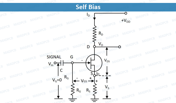
Self Bias Circuit
Since no gate current flows through the reverse-biased gate-source, the gate current IG=0 and, therefore, VG = iGRG =0.
With a drain current ID the voltage at the S is
VS = IDRS
The gate-source voltage is then
VGS = VG -VS = 0 – IDRS = -IDRS
So, voltage drop across resistance RS provides the biasing voltage VGg and no external source is required for biasing and this is the reason that it is called self-biasing.
The operating point (that is zero signal ID and VDS) can easily be determined from equation and equation given below:
VDS = VDD – ID(RD + RS)
Thus, DC conditions of JFET amplifier are fully specified. Self-biasing of a JEFT stabilizes its quiescent operating point against any change in its parameters, like transconductance. Let the given JFET be replaced by another JFET having the double conductance then drain current will also try to be double but since any increase in voltage drop across RS, therefore, gate-source voltage, VGS becomes more negative and thus increase in drain current is reduced.
Potential-Divider Bias
A slightly modified form of DC potential-divider bias is provided by the circuit shown in figure below. The resistor RG1 and RG2 form a potential divider across drain supply VDD. The voltage V2 across RG2 provides the necessary bias. The additional gate resistor RG1 from gate to supply voltage facilitates in larger adjustment of the DS bias point and permits use of larger valued RS.
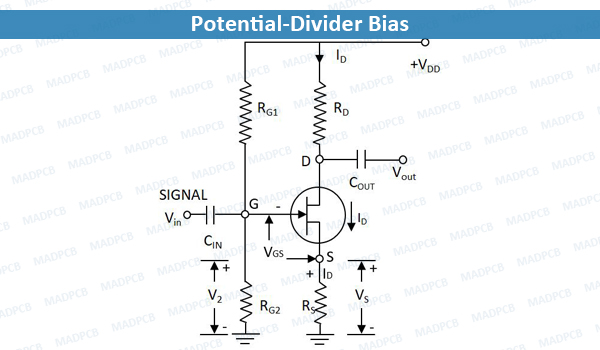
Potential-Divider Bias Circuit
The gate is reverse biased so that IG = 0 and gate voltage
VG = V2 = (VDD/R G1 + RG2)*RG2
And
VGS = VG – VS = VG -IDRS
The circuit is so designed that ID RS is greater than VG so that VGS is negative. This provides correct bias voltage.
The operating point can be determined as
ID = (V2 – VGS)/RS
And
VDS = VDD – ID(RD + RS)