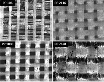
The tighter the weave netting, the more uniform the dielectric constant. Loose weaves resulting in less uniform dielectric constants in the PCB laminate can cause trace impedance variations and propagation skews in tightly matched signals, such as differential pairs that directly reference the weave. For example, on a sparse weaving such as glass style 106, one leg of the differential pair may be routed directly over a fiber weave while the other leg is routed between the fiber weaves. This results in a different εr for each leg of the differential channel.
In general, to counteract this skew, route traces at a small angle in a zig-zag fashion relative to the fiberglass strands to average out the number of on-weave and offweave traces. This technique requires more board routing room and may not be achievable in a space-constrained board. In this situation, select a more tightly woven glass style for the dielectric surrounding the high speed trace layers. Because more tightly woven glass styles add cost to the PCB, a good compromise is to select a medium woven glass style such as 2116 for the high-speed trace layers and a lower cost 106 or 1080 glass style for other lower-speed signal layers. For board design with ultra-high speed transceiver signals, we recommend to choose spread glass materials to mitigate this effect.

