What’s IoT?
The Internet of Things (IoT) describes physical objects (or groups of such objects) that are embedded with sensors, processing ability, software, and other technologies, and that connect and exchange data with other devices and systems over the Internet or other communications networks.
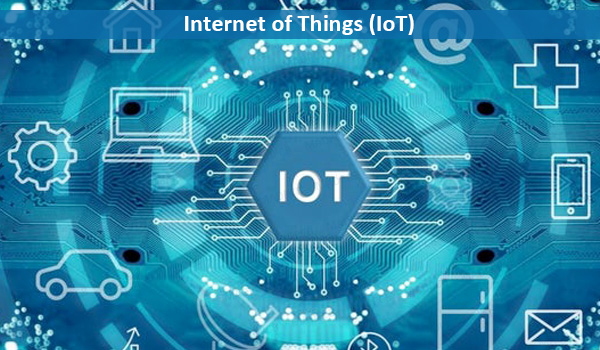
Internet of Things (IoT)
The field has evolved due to the convergence of multiple technologies, including ubiquitous computing, commodity sensors, increasingly powerful embedded systems, and machine learning. Traditional fields of embedded systems, wireless sensor networks, control systems, automation (including home and building automation), independently and collectively enable the Internet of things. In the consumer market, IoT technology is most synonymous with products pertaining to the concept of the “smart home”, including devices and appliances (such as lighting fixtures, thermostats, home security systems and cameras, and other home appliances) that support one or more common ecosystems, and can be controlled via devices associated with that ecosystem, such as smartphones and smart speakers. The IoT can also be used in healthcare systems.
There are a number of concerns about the risks in the growth of IoT technologies and products, especially in the areas of privacy and security, and consequently, industry and governmental moves to address these concerns have begun, including the development of international and local standards, guidelines, and regulatory frameworks.
History
The main concept of a network of smart devices was discussed as early as 1982, with a modified Coca-Cola vending machine at Carnegie Mellon University becoming the first ARPANET-connected appliance,[7] able to report its inventory and whether newly loaded drinks were cold or not. Mark Weiser’s 1991 paper on ubiquitous computing, “The Computer of the 21st Century”, as well as academic venues such as UbiComp and PerCom produced the contemporary vision of the IOT. In 1994, Reza Raji described the concept in IEEE Spectrum as “[moving] small packets of data to a large set of nodes, so as to integrate and automate everything from home appliances to entire factories”. Between 1993 and 1997, several companies proposed solutions like Microsoft’s at Work or Novell’s NEST. The field gained momentum when Bill Joy envisioned device-to-device communication as a part of his “Six Webs” framework, presented at the World Economic Forum at Davos in 1999.
The concept of the “Internet of things” and the term itself, first appeared in a speech by Peter T. Lewis, to the Congressional Black Caucus Foundation 15th Annual Legislative Weekend in Washington, D.C, published in September 1985. According to Lewis, “The Internet of Things, or IoT, is the integration of people, processes and technology with connectable devices and sensors to enable remote monitoring, status, manipulation and evaluation of trends of such devices.”
The term “Internet of things” was coined independently by Kevin Ashton of Procter & Gamble, later MIT’s Auto-ID Center, in 1999, though he prefers the phrase “Internet for things”. At that point, he viewed radio-frequency identification (RFID) as essential to the Internet of things, which would allow computers to manage all individual things. The main theme of the Internet of things is to embed short-range mobile transceivers in various gadgets and daily necessities to enable new forms of communication between people and things, and between things themselves.
Defining the Internet of things as “simply the point in time when more ‘things or objects’ were connected to the Internet than people”, Cisco Systems estimated that the IoT was “born” between 2008 and 2009, with the things/people ratio growing from 0.08 in 2003 to 1.84 in 2010.
IoT Opportunity Brings Opportunity to PCB Field
Now, the industry is all about creating an optimal IoT product that functions the same way no matter what form it takes in computers. It has become crucial to reimagine internal circuitry to reflect this change in methodology.
For the functionality and sustainability of new form aspects, printed electronics lead the way in making sophisticated manufacturing possible. Flex PCBs and high-density interconnect (HDI) PCBs provide the design freedom, cater to high-power demands in increasingly tightening circuit board spaces, are suitable for harsh environments and constant device stress, and offer high copper tensile strength.
Flex Printed Circuit (FPC) Advantages in IoT
Introducing flex PCBs dramatically reduces design limitations you might find with more rigid, traditional PCBs. Not only does a flexible board structure make way for revolutionizing the forms and shapes our electronics can take but also costs and errors can be reduced, thanks to the beneficial features of flex PCBs. Some of the best attributes of flex PCBs that make them suitable for IoT-focused designs include:
- Smaller size: The bulk of rigid PCBs limits design freedoms but also tends to require more space within the product. By occupying a reduced volume, flex circuits allow components like microphones, satellites and batteries to all fit in a small package without disrupting performance capabilities. Thin parts also permit flex PCBs to support denser circuitry.
- Lighter weight: With the lower space occupancy also comes weight savings of up to 95 percent. The option for lightweight internal components makes IoT devices much more versatile for all sorts of uses and environments, such as delicate surgical equipment or wearable hearing aids.
- Greater resistance: Flex PCB materials (like FCCL, coverlay) offer an improved level of durability, increasing their resistance to stress caused by impacts or vibrations. In industrial settings where the use of IoT PCBs is expanding, flex PCBs can stand up to harsher conditions. Similarly, with devices like fitness trackers, flex PCBs can resist errors caused by regular movement, body heat or humidity.
- Clearer wiring routes: Flex PCBs simplify wiring methods with their elimination of mechanical connectors. When imagining, for example, how the complexity of mechanics underneath the hood of a car can be improved for IoT functions, this simplified wiring becomes a valuable asset.
The flexible materials flex PCBs use as circuit connectors open up a world of possibilities for mobile devices and movable parts, making them an incredible tool for a wide range of IoT endeavors. If flexible printed circuit board novelties are on the horizon for you and your company, make sure to contact MADPCB for answers about the best flexible PCB materials for your industry and manufacturing quotes.
To accommodate smaller spaces made possible by flex PCBs, HDI PCBs are here to offer the highest board density for optimal circuit performance.
HDI PCB Benefits in IoT
As a frontrunner for the small-packaged designs we see in personal electronics today, high-density interconnect (HDI) PCBs are an indispensable tool. Designers and manufacturers alike need to consider the benefits of these boards, including their speed and reliability, when facing the big picture of the IoT head-on. Some of the most optimal aspects of HDI PCBs in light of IoT include:
- Reduced size and weight. HDI PCBs are known for their dense component placement. They are characterized by tinier trace widths and superior wiring density, thanks to stacked microvias and other features that help save board space. Smaller boards mean a greater number of uses, making them ideal for use with the ever-changing strategies of the IoT.
- Cleaner circuit route. HDI boards grant versatile routing options thanks to blind or buried vias and microvias that smooth dense parts of the circuit. Additionally, designers can replace through-holes with microvias, which, along with the shorter distances between components, improves signal integrity. Top performance in small spaces makes HDI PCBs crucial for IoT optimization.
- Improved cost-effectiveness. Higher energy-efficiency and a reduced need for layering lead to a product that is more cost-effective to both implement and produce. The smaller size also permits the use of fewer materials to create a functional board.
The most frequent use for HDI boards involved the benefit of their miniature size advantages and the reliability they offer for creating smart IoT devices. The density of their circuits can mean you will want to only trust a highly experienced supplier with your HDI PCBs because of the need for extra-delicate care in their manufacture.
Whatever your use for high-density interconnect PCBs may be, you can learn more about MADPCB‘s quick quote services to find the printed circuit boards to suit your needs.